With the increasing popularity of automotive start-stop technology (auto-off when the engine is idle), more and more automotive systems must operate at low input voltages. This type of low input voltage can occur during warm start (at which point the battery voltage can drop up to 6V) and cold start (at which point the battery voltage can drop up to 3V). This article describes an intermediate voltage 8V switching power supply that can withstand the full input voltage range of the car, including cold start and load dump conditions. The power supply guarantees a stable 8V power supply for common subsystems such as CD drives, LCDs, and radio modules in modern infotainment systems. In order to avoid AM and FM band interference, the switching power supply operates at a fixed frequency of 2MHz, making it an ideal solution for radio systems.
Importance of low input voltage capability and EMI requirements
Figure 1 shows a common automotive system that requires different architectural solutions.
In a system with a mains supply of 3.3V, a front-end buck converter with low dropout voltage can meet the requirement (Case 1). In addition, the boost converter can operate at 3.3V and can be adjusted to 5V (for CAN bus transceivers, for example) or other higher voltages (case 2). Systems operating at 5V or higher rails require a “pre-boosting†front-end to ensure that the input voltage to the buck converter does not drop below the specified voltage (Case 3).
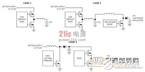
Figure 1 Automotive Power Solutions
Low electromagnetic emissions (EMI) are also a key requirement for automotive power supplies, especially in the sensitive AM band. The switching converter designed in this work is designed to operate above the AM band, that is, the frequency is guaranteed to be higher than 1.71 MHz (the upper part of the medium wave) to meet this requirement, so that the switching converter can be operated at high frequencies and external passive components can also be reduced. Size and cost.
Key Design Parameters of Automotive Switching Power SuppliesFigure 2 shows the switching power supply schematic. The power supply includes a 4.5V to 40V boost controller (IC1) and a 36V step-down controller (IC2), as well as additional circuitry for proper operation. The two ICs are synchronized to an external 2MHz square wave logic signal, which is provided by a microcontroller or a dedicated IC. This method gives great flexibility in choosing the optimal switching frequency for the power supply. During normal operation of the battery, disable the IC1 and IC2 regulators to stabilize the OUTB node voltage at 8V. When the battery voltage drops during a cold start, IC1 is enabled and the voltage at the OUTA node is raised. This allows IC2 to stabilize the OUTB node voltage at 8V. Due to the high reliability of the two ICs, the entire design can withstand car dump loads up to 40V. The system is configured and tested with its main output (OUTB) providing 20W of power (), and even higher output power can be provided after modifying external components. (See below for a discussion of the optimal external components for IC1 and IC2.)
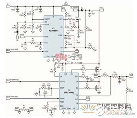
Figure 2 Switching power supply schematic includes boost controller (IC1, MAX15005) and buck controller (IC2, MAX16952)
External Components Optimize IC2 Performance
Output voltage and switching frequency
To adjust the 8V voltage at the OUTB node, the correct feedback resistor divider (made up of resistors R22 and R21) must be selected. Note that IC2's data sheet recommends a low side resistance of less than 100kΩ. To select the 51kΩ low-side resistor divider for R22, the high-side resistor divider must be selected according to Equation 1:

(Formula 1)
In the formula, VFB = 1V (typical).
Select the standard resistor value of 360kΩ for R21. The typical output voltage value produced is:

(Formula 2)
Assuming that the resistor tolerance is 1%, the minimum and maximum voltage values ​​(OUTB) for the entire switching power supply are:

(Formula 3)

(Formula 4)
In the formula, VFB(MIN) is 0.985V, VFB(MAX) is 1.015V.
According to the data sheet, the external frequency must be higher than 110% of the frequency selected within the IC. Since we are synchronizing the switching frequency of IC2 with the external 2MHz signal, we chose the internal oscillator resistor R16 to set the internal switching frequency below 1.8MHz. For this reason, we chose a 30kΩ resistor for R16. In order to switch IC2 at a fixed frequency of 2MHz, differential pressure conditions must be avoided. The IC avoids dropout voltages until the off-time (tOFF) is longer than 100ns (typical). This means that the maximum duty cycle of the system must not exceed:

(Formula 5)
Considering that the efficiency (Eff) of the buck regulator IC2 is 90%, the minimum input voltage (OUTA) of the 2MHz fixed frequency switch can be ensured to be:

(Formula 6)
This means that the OUTA voltage must not fall below the 11.11V threshold. To ensure that the OUTA voltage is always higher than 11.11V and the battery voltage (IN node) is lower than 11.5V, IC1 must be enabled. This leaves a margin of approximately 390mV for the voltage drop across inductor L1 and Schottky diode D2.
During the 40V load dump spike, OUTA voltage reaches its high voltage and IC2 must stabilize its output at 8V. So, during the load dump spike, IC2's duty cycle should be:

(Formula 7)
The device's minimum on-time (tON) is 80ns (typ), making it possible to achieve a minimum duty cycle of:

(Equation 8)
Switching frequency is 2MHz.
The minimum 0.16 duty cycle ensures 8V regulation during 40V load dump.
Inductance and current detectionIf you reduce the inductor peak current by using a large inductor value, you can increase the efficiency of IC2. However, achieving this requires a larger printed circuit board (PCB) area and degrades load regulation. As an acceptable trade-off, the inductor value can be selected such that LIR (the ratio of the peak-to-peak current of the inductor to the average current of the DC) is equal to or less than 0.3. Consider the following equation with reference to Figure 3:
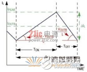
Figure 3 Inductor current of IC2 (MAX16952)

(Formula 9)

(Formula 10)

(Formula 11)
Combine these formulas and get the formula to calculate the L value:

(Formula 12)
Therefore, the minimum inductance value that achieves a LIR factor of 0.3 or less under normal conditions (OUTA = 12V) is:

(Formula 13)
L2 uses a standard inductor of 2.2μH. The resulting LIR factor is 0.24. The peak inductor current is:

(Equation 14)
The current limit is triggered when the voltage on the R20 sense resistor reaches 68mV (minimum). Leave some margin for the inductance tolerance, so that the voltage drop of the sense resistor is 60% of the current limit threshold when the inductor current reaches the peak value (IPEAK), so as to determine the size of the sense resistor:

(Expression 15)
Therefore, choose a standard resistance of 15mΩ for R20.
Optimize the external components of IC1
UVLO threshold
The first step in selecting external components for boost converter IC1 is to determine the external undervoltage lockout (UVLO) threshold by selecting the resistor divider connected between the main input IN pin, the ON/OFF pin, and ground. For this design, we turn off the device when the input voltage is below 5V; assume a higher voltage during the cold start phase. After selecting a 100kΩ resistor for R5, use Equation 16 to select the R4 resistor value:

(Expression 16)
So choose a standard resistance of 300kΩ for R4.
Overvoltage input (OVI)
As discussed above for IC2, we must ensure that the OUTA node voltage is not lower than 11.11V so that the buck controller does not exceed the regulation range. Considering this voltage threshold and adding a reasonable voltage drop for inductor L1 and diode D2, IC1 must conduct when the IN voltage drops below 11.5V. However, to optimize efficiency, IC1 must not operate when the battery voltage is normal (IN = 12V).
To achieve this, IC1 is enabled or disabled according to the main power supply using a resistor divider connected between the IN pin, OVI pin, and ground. Therefore, when the voltage on the OVI pin exceeds the 1.228V threshold, IC1 is disabled; when the OVI pin voltage drops to 1.228V, IC1 turns on, typically with a hysteresis of 125mV. Select the low-side R2 resistor divider equal to 20kΩ. Consider that IC1 should turn off when the input voltage rises above 11.6V. You must select the high-side R1 resistor divider according to Equation 17:

(Equation 17)
With a standard 170kΩ R1 resistor, IC1 is disabled when the supply voltage rises above 11.67V. This maintains a 330mV headroom for a nominal 12V IN battery voltage. Taking into account the hysteresis on the OVI comparator, we can estimate the main supply voltage drop that enables IC1:

(Equation 18)
This result proves that the hysteresis is too large. We will definitely lower it down so that the voltage drop threshold at the main power supply is at least 11.5V, which can be achieved by adding series resistors and Schottky diodes (R3 and D1) between the OVI pin and the SS pin. When IC1 is disabled, the SS pin is internally connected to ground and R3 and R2 are connected in parallel, effectively reducing hysteresis. R3 uses a 180kΩ resistor, ignoring the diode drop, and the new voltage drop threshold on the main supply becomes:

(Expression 19)
With this configuration, it is possible to reach the target threshold at the rising and falling edges of the input voltage. Note that if feasible, another alternative is to use an external comparator to monitor the main power and directly drive the OVI input pins.
The output voltage
To maintain the 2MHz fixed switching frequency, as described in the IC1 data sheet, the minimum tON of 170ns must be considered under all application conditions. The smallest tON causes a minimum duty cycle of 34% (with a 2MHz switching frequency), which limits the IC's adjustable minimum output voltage. See Figure 4. To estimate this voltage threshold, the duty cycle formula of the boost regulator must be considered:

(Equation 20)
The input voltage (VIN) is the maximum (11.67V in this design) and IC1 operates with minimum duty cycle. By rewriting Equation 20, the minimum regulated output of IC1 under this limit condition can be estimated:

(Equation 21)
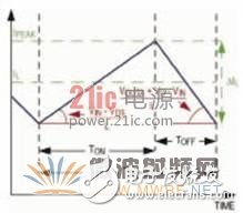
Figure 4 IC1 (MAX15005) inductor current
The above calculation conditions are the minimum duty cycle and the maximum input voltage, taking into account the voltage drop across the Schottky diode D2 of 0.3V, and neglecting the voltage drop across the NMOS N1. Therefore, IC1 must adjust the output voltage above 17.38V to ensure that the switching frequency is 2MHz under all operating conditions.
The high-side feedback resistor divider R14 can be calculated by selecting the 10kΩ resistor for the low-side feedback resistor divider R13:

(Expression 22)
In the formula, VFB(MIN) = 1.215V.
Finally, R14 uses a 1%-tolerance 137kΩ resistor, and IC1 regulates the minimum output voltage to be:

(Equation 23)
This ensures that the switching frequency of IC1 is always fixed at 2MHz.
Assuming that the output power of the design is equal to 20W (), and the efficiency of IC2 is 90%, the output power of IC1 must be at least 22.3W. Therefore, taking into account the 17.53V regulation output voltage, IC1's average output current is 1.27A. When IC1 is used to regulate higher output voltages, the output current is reduced, requiring a low cost D2 Schottky diode. However, the output capacitor C7 must be able to withstand the output voltage regulated by IC1 itself.
Synchronization and maximum duty cycle
To ensure external synchronization of the IC1 switching frequency, the frequency must be at least 102% higher than the set internal oscillator frequency. Select a 7kΩ resistor for R6 and a 100pF capacitor for C4. IC1's internal oscillator frequency is approximately 1MHz, allowing an external synchronization frequency of 2MHz.
When the SYNC input detects the rising edge of the sync signal, capacitor C4 discharges through the internal 1.33mA (typ) current source. When the voltage on this capacitor (RTCT pin) reaches 500mV, capacitor C4 is charged through R6 connected to the VREG5 pin until the rising edge of the next synchronization signal is detected. The discharge time (TDISCHARGE) determines the minimum tOFF of the regulator. If this time is less than 160ns (as in this example), the minimum tOFF clamp is 160ns. In fact, assuming a charge time (TCHARGE) of 340ns (TP = 500ns), the voltage on RTCT increases:

(Equation 24)
Considering that the net discharge current in the discharge phase is 615μA1, the discharge time of the increased voltage on the RTCT pin is equal to:

(Equation 25)
The 160ns minimum tOFF means that the maximum duty cycle is 68%. Again applying the boost regulator duty cycle equation to this example (Equation 20) requires a maximum duty cycle (lower input voltage, 5V in this example), IC1 regulates the maximum voltage on the OUTA pin to:

(Formula 26)
This voltage value ensures that IC2 does not operate in differential pressure conditions.
Inductor selection
The minimum output current of the boost regulator constrains the choice of inductor value. To ensure that the regulator IC1 always operates in continuous mode, the minimum inductance is:

(Equation 27)
In this design, the worst-case condition is that when VIN is at its maximum value (11.67V), the corresponding duty cycle is 37%.
When the minimum current of the 8V node is 1A and the efficiency of the buck converter IC2 is 90%, the minimum output power of the buck regulator becomes 9.44W. This power corresponds to the 538mA minimum output current, IOUTA(MIN), which is sourced by the boost regulator. Taking these conditions into account, the solution of Equation 27, the minimum inductance is 1.32μH. For this design, choose a 2.2μH inductor for L1.
Current Detection
When the voltage across the sense resistor reaches a typical value of 305mV, IC1's current limit is triggered. Therefore, to properly select this resistor, the peak current in the boost inductor must be calculated:

(Equation 28)
The peak value occurs when the input voltage is at its minimum value. In this example, 5V, the maximum duty cycle is 68%. As calculated in Equation 26, the boost output voltage (OUTA pin) is 15.32V and requires 1.46A of IOUTA current to provide IC2 with the necessary power. In the worst case, the peak inductor current is 4.95A. To maintain proper headroom, the sense resistor is designed to have a 200mV drop across the peak inductor current.

(Equation 29)
Therefore, select 40 MΩ resistor for R10.
lab testingCold start test
Cold start tests were performed in the laboratory. The forced mains voltage (IN) drops from 12V to 7V within 10ms. As shown in Figure 1, when the IN voltage drops, IC1 starts to raise the voltage of OUTA to 17.5V. This allows IC2 to regulate the OUTB voltage to 8V. On the other hand, when the input voltage returns to its operating value, IC1 stops operating, OUTA voltage drops to IN voltage, and there is a small voltage drop across diode D2 and inductor L1. For each test, the output load on the OUTB pin is 2.5A.
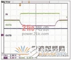
figure 1
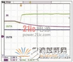
figure 2
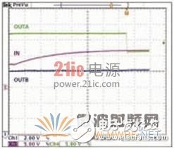
image 3
Figures 2 and 3 show the amplified cold start voltage drop and rise phases, respectively.
Analyze the frequency domainWith the help of the oscilloscope's embedded FFT tool, the frequency spectrum of IC2's switching node LX_Buck pin voltage during cold start is shown in Figure 4 (IN voltage drop) and Figure 5 (IN voltage rise). Note that the spectrum includes the 2MHz frequency, the corresponding harmonics, and of course the DC component. There is no AC component below 2 MHz, thereby preventing noise interference in the AM band.
The same process is performed on IC1's switch node LX_Boost. The test results in Figure 6 and Figure 7 show 2MHz frequency, harmonics, and DC components, eliminating AM band noise.
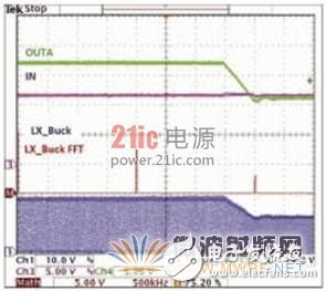
Figure 4
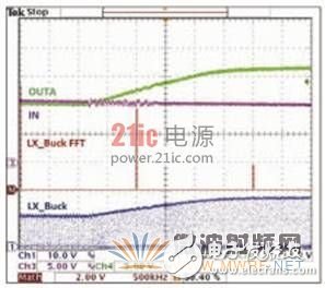
Figure 5
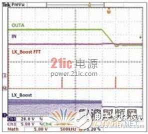
Figure 6

Figure 7
Optional design improvementsTo optimize efficiency, the designer can bypass the Schottky diode D2 if the boost regulator IC1 is not operating under normal application conditions. When the main power supply is normal, an n-channel MOSFET can be connected in parallel with D2 to achieve this purpose. To reduce electromagnetic interference (EMI), slow down the voltage edge on the MOSFET gate and increase the external resistance (R8, R17, R18, and R19). This will increase power consumption. To filter spikes in the IC1 current detection waveform, it is useful to add a small RC filter (C6 and R9). By increasing the offset to the R7 resistor, the current-limit threshold of IC1 can also be reduced. This will reduce power consumption on the sense resistor R10.
Fast Recovery Diode is a semiconductor device which possesses short reverse recovery time for rectification purpose at high frequency. A quick recovery time is crucial for rectification of high-frequency AC signal. Diodes are mostly used in rectifiers because they possess ultra-high switching speed.
Fast Recovery Diode,Fast Recovery Rectifier Diode,Super Fast Recovery Diode,Fast Recovery Epitaxial Diode,Recovery Diode
YANGZHOU POSITIONING TECH CO., LTD. , https://www.pst-thyristor.com