This article is mainly about the related introduction of CC1000 circuit, and focuses on the connection diagram of the radio frequency CC1000 circuit and elaborates it in detail.
CC1000CC1000 is an ideal UHF monolithic transceiver communication chip manufactured in 0.35μm CMOS process based on Chipcon's SmartRF technology. Its operating frequency band is 315, 868 and 915MHz, but CC1000 can be easily programmed to work in the range of 300-1000MHz. It has low voltage (2.3~3.6V), extremely low power consumption, programmable output power (-20~10dBm), high sensitivity (generally -109dBm), small size (TSSOP-28 package), integrated bit synchronizer Features. Its FSK data transmission can reach 72.8Kbps, with 250Hz step length programmable frequency capability, suitable for frequency hopping protocol; the main operating parameters can be programmed and changed through the serial bus interface, and it is very flexible to use.
Three-wire serial data port
CC1000 can be programmed through a simple three-wire serial interface (PDATA, PCLK, and PALE). There are 36 8-bit configuration registers, each addressed by a 7-bit address. A complete CC1000 configuration requires 29 data frames to be sent, each with 16 bits (7 address bits, 1 read/write bit and 8 data bits). The PCLK frequency determines the time required for full configuration. Under the PCLK frequency of 10MHz, the time required to complete the entire configuration is less than 60μs. In the low-potential mode setting, only one frame needs to be transmitted, and the required time is less than 2μs. All registers are readable. In each write cycle, 16-bit bytes are sent to the PDATA channel, and the 7 most important bits (A6:0) in each data frame are the address bits, and A6 is the MSB (the most significant bit), which is sent first. The next bit to be sent is the read/write bit (high level write, low level read). During the transmission address and read/write bit period, PALE (program address latch enable) must remain low, and then transmit 8 One data bit (D7:0), as shown in Figure 3. Table 1 is a description of each parameter. PDATA is valid on the falling edge of PCLK. When the last byte of the 8-bit data bit, D0, is loaded, the entire data word is loaded into the internal configuration register. The configuration information programmed in the low-potential state is valid, but the power cannot be turned off.
The microcontroller can also read the configuration register through the same interface. First, send the 7-bit address bit, and then the read/write bit is set to low level to initialize the data read back. Then, CC1000 returns data from the addressing register. At this time, PDATA is used as an output port. During the read-back data period (D7:0), the microcontroller must set it to tri-state, or set it to a high level when the pin is open.
CC1000 adopts phase-locked loop technology. The transmission frequency is configured by the internal frequency synthesizer. The configurable range is 300~1000MHz. It is suitable for the application of frequency hopping protocol. Generally, 10 or 20 frequency points can be configured. The sensitivity of this chip is ï¼109dBm, and can be automatically calibrated, the programmable output power is ï¼20dBm~+10dBm, and the communication rate can reach 78.6Kbps.
The main working parameters of CC1000 can be programmed by a serial interface, which is very convenient and flexible to use. The CC1000 chip has fewer peripheral components, and does not require high precision, and provides three encoding methods to interface with the microcontroller. So CC1000, a microcontroller and a few external components can form a complete RF transceiver system.
RF CC1000 circuit connection diagram analysis
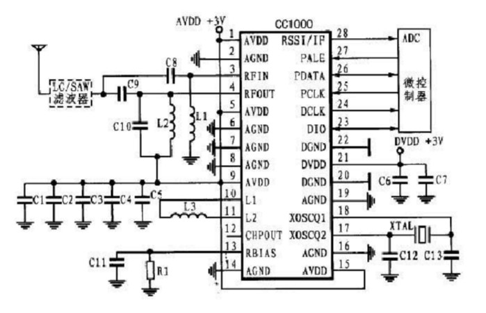
The figure above is a typical application circuit of CC1000. Adjusting the parameter values ​​of components C1-C13, L1-L3, R1 can make
CC1000 works at different operating frequencies (300~1000MHz).
The microcontroller can set up the CC1000 through the CC1000's serial interface (PDATA, PAlE, and PCLK), and complete the data reception and transmission through the CC1000's DIO.
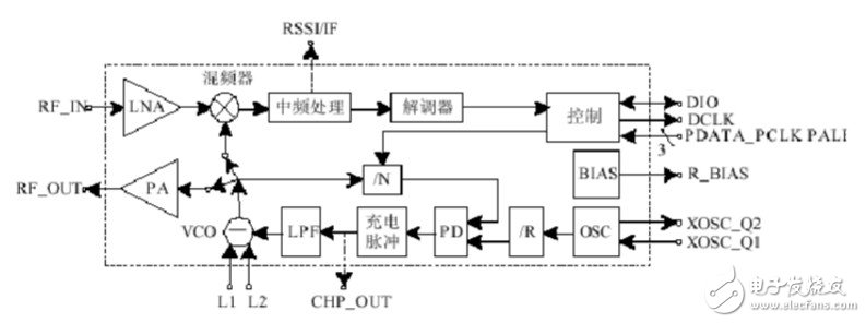
Figure 1 shows a simplified block diagram of the cc1000. In the receiving mode, the cc1000 can be regarded as a traditional superheterodyne receiver. The radio frequency (RF) input signal is amplified by a low noise amplifier (LNA) and flipped into the mixer. The intermediate frequency (IF) signal is generated by mixing the RF input signal into the mixer. In the intermediate frequency processing stage, the signal is amplified and filtered before it is sent to the demodulator. The optional RSSI signal and IF signal can also be generated by mixing the RSSI/IF pin. After demodulation, the CC1000 outputs the demodulated digital signal from the pin DIO, and completes the synchronization of the demodulated signal through the clock signal provided by the PCLK on the chip.

In the transmission mode, the output signal of the voltage controlled oscillator (VCO) is directly fed to the power amplifier (PA). The RF output is controlled by the data added to the DIO pin, called FSK. This internal T/R switching circuit makes the design of antenna connection and matching easier. it
The local oscillator generated by the frequency synthesizer is fed to the power amplifier in the receiving state. The frequency synthesizer is composed of crystal oscillator (XOSC), phase detector (PD), charging pulse, VCO and frequency divider (/R and /N). The external crystal must be connected to the XOSC pin, and only the external inductor needs to be connected to the VCO. (2) Application circuit
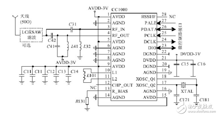
When the cc1000 is working, there are very few external components. The typical application circuit is shown as in Fig. 2. When configuring different cc1000 transmission frequencies, the parameters of the peripheral components are also different.

Table 1 Serial interface timing description

The microcontroller can also read the configuration register through the same interface. First, send the 7-bit address bit, and then set the read/write bit to low level to initialize the read data. Next, the cc1000 returns data from the addressable register. At this time, PDATA is used as an output port, and the microcontroller must set it to three states during readback (D7:0), or set it to high when the pin is turned on. The time of the read operation is shown in Figure 4.

Connect with microcontroller
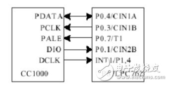
The microcontroller uses 3 output pins for the interface (PDATA, PCLK, PALE), and the pin connected to PDATA must be a bidirectional pin for sending and receiving data. The DCLK that provides data timing should be connected to the input of the microcontroller, and the remaining pins are used to monitor the LOCK signal (at the pin CHP_OUT). When the PLL is locked, this signal is logic high. Figure 5 is a schematic diagram of the interface between the P87LPC762 microcontroller and CC1000.

That's it for the related introduction of the radio frequency CC1000 circuit connection diagram. If there are any deficiencies, please correct me.
Related reading recommendations: Understand FSK technology and CC1000-based RF optical transmission design
Related reading recommendations: cc1000 wireless module circuit diagram
Piezoelectric ceramic are a ferroelectric compound. This means, that the electro-mechanical conversion process for producing a motion is related a kind of self-enhancement process based on an internal reorganization of the material's structure. This self-enhancement process results in the higher piezoelectrical efficiency of PZT when compared to natural materials like quartz.
Piezoelectric ceramic are generally manufactured from PZT (Pb - lead, Zr - zirconium, Ti - titanium). The PZT- formulation can be varied with a variety of dopants allowing for a broad spectrum of material properties optimized for different application profiles.
Yuhai Company is able to manufacture piezoelectric ceramic elements in a wide range of shapes and sizes. piezoelectric discs, piezo rings, piezo plates, and piezo tubes (cylinders) is the main shapes Yuhai Company most frequently manufactures, we also have a great deal of experience manufacturing hemispheres, trapezoids and other customized shapes.
If the listed shapes and sizes was not the elements you are looking for, please contact us for more information. We can work with you to create the correct shape and size for you.Piezoelectric Elements,Piezo Ceramic Disc,Piezoelectric Ceramic Discs,Pzt Element
Zibo Yuhai Electronic Ceramic Co., Ltd. , https://www.yhpiezo.com