The specific analysis details of this circuit are described below.
(1) The negative half-cycle large-scale signal output from the 1 pin of integrated circuit A1 will not cause VT1 overcurrent, because the negative half-cycle signal will only lower the base voltage of the NPN transistor, and the base current will decrease, so there is no need to add negative Half-cycle limiting circuit.
(2) The above description is a unidirectional limiting circuit. This limiting circuit can only limit the signal part of the positive half cycle or the negative half cycle of the signal, and the signal of the other half cycle is not limited. The other is a two-way limiting circuit that limits the positive and negative half-cycle signals simultaneously.
(3) The cause of abnormal increase in signal amplitude is various. For example, accidental factors (such as fluctuations in power supply voltage) cause the signal amplitude to increase a lot at a certain moment, and the external large-scale interference pulse intrusion circuit also causes a signal. A common cause of abnormal increase in a moment.
(4) After the three diodes VD1, VD2 and VD3 are turned on, the sum of the DC and AC voltages on the pin 1 of the integrated circuit A1 is 2.1V. This voltage is applied to the VT1 base through the resistor R1, which is also the highest VT1. The base voltage, at which point the base current is also the maximum base current of VT1.
(5) Since the 1st and 2nd external circuits of the integrated circuit A1 are the same, the limiting protection circuit in the external circuit works in the same principle, and only one circuit can be analyzed when analyzing the circuit.
(6) According to the characteristics of the series circuit, the currents in the series circuit are equal, so that it can be known that the three series diodes of VD1, VD2 and VD3 are turned on at the same time, otherwise they are cut off at the same time, and there will never be a certain one in the series circuit. The phenomenon that the diode is turned on and some diodes are turned off. 4.4 Fault Detection Method and Circuit Fault Analysis The diode fault detection in this circuit mainly uses the multimeter ohmmeter to measure the forward and reverse resistance of the circuit. Because the diode in this circuit does not work in the DC circuit, it is adopted. The method of measuring the DC voltage drop across the diode is not suitable. Diodes in this circuit are less likely to fail because they operate in a small signal state. If there is an open circuit fault in one of the diodes in the circuit, the circuit will have no limiting effect, which will affect the normal operation of the latter circuit.
5 diode switch circuit and fault handling
The switch circuit is a commonly used function circuit, such as a switch in a lighting circuit in a home, a power switch in various household appliances, and the like. There are two main types of switches in the switching circuit:
(1) Mechanical switch, using mechanical switch components as components in the switch circuit.
(2) Electronic switches, so-called electronic switches, do not use mechanical switching devices, but use diodes, transistors and other devices to form a switching circuit.
5.1 Switching Diode Switching Characteristics Description
The switching diode is the same as a normal diode and is also a PN junction structure. The difference is that the switching characteristics of this diode are required. When a forward voltage is applied to the switching diode, the diode is in an on state, which is equivalent to the on state of the switch;
When a reverse voltage is applied to the switching diode, the diode is in an off state, which is equivalent to the off state of the switch. The on and off states of the diode complete the on and off functions.
Switching diodes use this characteristic, and through the manufacturing process, the switching characteristics are better, that is, the switching speed is faster, the junction capacitance of the PN junction is smaller, the internal resistance at the time of conduction is smaller, and the resistance at the time of turning off is large. As shown in Table 5.1, the concept of switching time is explained.
Table 5.1 Concept of switching time concept

5.2 Typical Diode Switch Circuit Working Principle
Diodes consist of a variety of electronic switching circuits, as shown in Figure 5.1, which is a common diode switching circuit.
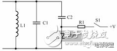
Figure 5.1 Diode Switch Circuit
By observing this circuit, you can familiarize yourself with the following aspects to facilitate the analysis of the working principle of the circuit:
(1) Understanding the function of this unit circuit is the first step. It can be seen from the circuit shown in Figure 8-14 that the inductor L1 and the capacitor C1 are connected in parallel. This is obviously an LC parallel resonant circuit, which is the basic function of this unit circuit. After this is clear, other components in the circuit can be known. It should be an auxiliary component around this basic function, which is an extension or supplement to the basic functions of the circuit. This idea can easily analyze the role of components in the circuit.
(2) C2 and VD1 form a series circuit, and then parallel with C1. From this circuit structure, a judgment result can be obtained: the function of the branch of C2 and VD1 is to change the total of the parallel connection with the capacitor C1 through the branch. The size of the capacity, the reason for this judgment is: the total capacitance of the C2 and VD1 branches in parallel with C1 is changed, and the oscillation frequency of the LC parallel resonant circuit composed of L1 is changed. Therefore, this is a circuit that changes the frequency of the LC parallel resonant circuit.
The following is a summary of the analysis of the diode electronic switch circuit:
(1) In the circuit, C2 and VD1 are connected in series. According to the characteristics of the series circuit, C2 and VD1 are either connected to the circuit at the same time or disconnected at the same time. If only C2 is required to be connected in parallel on C1, C2 can be directly connected in parallel to C1, but serially connected to diode VD1, indicating that VD1 controls the access and disconnection of C2.
(2) According to the on and off characteristics of the diode, it is known that VD1 is turned on when the C2 access circuit is required, and VD1 is turned off when the C2 access circuit is not required. This mode of operation of the diode is called a switching mode. The circuit is called a diode switch circuit.
(3) The diode should be turned on and off to have voltage control. In the circuit, the positive electrode of VD1 is connected to the DC voltage +V terminal through the resistor R1 and the switch S1. This voltage is the control voltage of the diode.
(4) The switch S1 in the circuit is used to control whether the operating voltage +V is connected to the circuit. According to the S1 switching circuit, it is easier to confirm that the diode VD1 is operating in the switching state, because the opening and closing of the S1 controls the conduction and the off of the diode. Table 5.2 shows the working principle of the diode electronic switch circuit.
Table 5.2 Description of the working principle of the diode electronic switch circuit
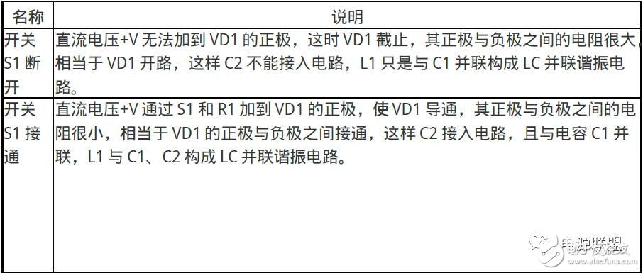
In the above two states, due to the difference in capacitance in the LC parallel resonant circuit, one case is only C1, and the other case is that C1 is connected in parallel with C2, and the resonant frequency of the LC parallel resonant circuit is different under different capacitances. Therefore, the real role of VD1 in the circuit is to control the resonant frequency of the LC parallel resonant circuit.
Details on the analysis of the diode electronic switching circuit are as follows:
(1) When there is a switch component in the circuit, the analysis of the circuit takes the two cases of the switch on and off as an example, and analyzes the working state of the circuit separately. Therefore, when a switching element appears in the circuit, it can provide an idea for circuit analysis.
(2) The signal in the LC parallel resonant circuit is applied to the positive electrode of VD1 through C2, but since the amplitude of the signal in the resonant circuit is relatively small, the amplitude of the positive half cycle applied to the positive terminal of VD1 is small, and VD1 is not turned on.
5.3 Fault Detection Method and Circuit Fault Analysis
Figure 5.2 shows the wiring diagram when switching the diode in the detection circuit. When the switch is turned on, the DC voltage drop across the diode VD1 should be 0.6V. If it is much smaller than this voltage, the VD1 is short-circuited. If it is farther than this voltage value. Explain that VD1 is open. In addition, if it is not obvious that VD1 has a short circuit or open circuit fault, you can use the multimeter ohmmeter to measure its forward resistance, which is small, otherwise the forward resistance is not good.
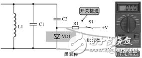
Figure 5.2 Wiring diagram of the switching diode in the detection circuit
If the switching diode in this circuit is open or shorted, the oscillation frequency cannot be adjusted. When the switching diode is open, the capacitor C2 cannot be connected to the circuit. At this time, the oscillation frequency is increased. When the switching diode is short-circuited, the capacitor C2 is always connected to the circuit, and the oscillation frequency is lowered.
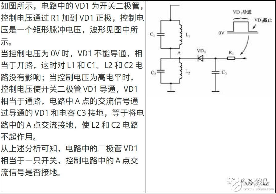
5.4 Analysis of the working principle of similar circuits
6 diode detection circuit and fault handling
Figure 6.1 shows the diode detection circuit. VD1 in the circuit is a detector diode, C1 is a high frequency filter capacitor, R1 is the load resistance of the detector circuit, and C2 is a coupling capacitor.
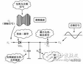
Figure 6.1 Diode Detector Circuit
6.1 Circuit Analysis Preparation Knowledge
As we all know, the radio has two kinds of AM radio and FM radio. The AM signal is the signal processed and amplified in the AM radio. See the schematic diagram of the amplitude modulation signal waveform in the figure. The following points are mainly explained for this signal waveform:
(1) From the amplitude modulation radio antenna is the amplitude modulation signal.
(2) The middle part of the signal is a carrier signal with a very high frequency. Its upper and lower ends are the envelope of the amplitude modulation signal, and its envelope is the required audio signal.
(3) The upper envelope signal and the lower envelope signal are symmetrical, but the signal phase is opposite. The radio finally needs only the upper envelope signal, the lower envelope signal is not used, and the middle high frequency carrier signal is not needed. 6.2 Description of the functions of each component in the circuit
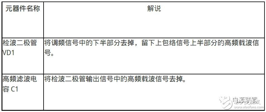
As shown in Table 6.1 is the component role explanation.

6.3 Analysis of the working principle of the detector circuit
The detection circuit is mainly composed of a detection diode VD1.
In the detection circuit, the amplitude modulation signal is applied to the positive pole of the detection diode. At this time, the working principle of the detection diode is basically the same as that of the rectifier diode in the rectifier circuit. The amplitude of the signal is used to turn on the detection diode, as shown in Figure 6.2. Schematic diagram of the waveform after it has been expanded.
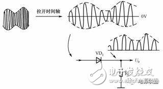
Figure 6.2 Schematic diagram of time-axis expansion of amplitude modulation waveform
As can be seen from the unfolded amplitude modulated signal waveform, it is an AC signal, but the amplitude of the signal is changing. This signal is applied to the positive pole of the detector diode. The positive half-cycle signal turns on the diode, and the negative half-cycle signal turns off the diode. This is equivalent to the operation of the rectifier circuit. The envelope of the positive half-cycle signal is obtained on the detector diode load resistor R1. The dotted line is shown in the waveform of the output signal of the detector circuit (the output signal waveform when no high-frequency filter capacitor is added).
The output signal of the detector circuit is composed of three signal components: audio signal, DC component and high-frequency carrier signal. The detailed circuit analysis needs to be developed according to the three signal conditions. The most important of these three signals is the analysis and working principle of the audio signal processing circuit.
(1) The required audio signal, which is the envelope of the output signal, as shown in Figure 6.3. This audio signal is coupled to the output capacitor C2 of the detector circuit and sent to the subsequent circuit for further processing.
Solder Cup Waterproof D-Sub Connector
The Solder Cups D-sub connector, also known as Solder Cups D-sub connector , typically contains a pin layout of 9 pin, 15 pin, 25 pin, 37 pin & 50 pin positions housed in increasing shell sizes accordingly. They are available in both male (plug) and female (socket) variants with the male signal contacts/pins (current rating of 5A) spaced every 2.76mm in horizontal rows and the spacing of rows vertically at 2.84mm laid out half the distance between pins of existing rows.
IP66 IP67 Rated Waterproof D-Sub Panel Mount Solder Connectors
Harsh outdoor or indoor environments can destroy electronic equipment. Standard D-sub connectors are not intended to withstand contaminants such as water and dust. These waterproof solder cup connectors are available in male or female genders and DB9, DB15, DB25, and HD15 sizes. They will accommodate wire ranges from 30 - 20 AWG. Construction features gold plated brass contacts, nickel plated steel shells, and a silicone insulating ring. Maximum recommended panel thickness is 0.078".
Antenk offer a wide range of waterproof standard density and high density male and female high density D-Sub connectors solder cup with stamped and formed Contacts in cable mount used in a variety of demanding applications.
Antenk's Solder Cup D-Sub Connectors Stamped contacts
FEATURES
Solder cup d-subs available in industry sizes/positions
Low cost economy series.
Nickel shells have indents to provide grounding and additional retention.
Low cost & high performance, non-removable stamped contacts.
Optional mounting hardware available.
Antenk's SOLDER CUP D-SUB CONNECTORS Stamped contacts
MATERIALS
Shell: Steel, Tin or Nickel Plated
Insulator: Glass-filled thermoplastic. U.L. rated 94V-O
(230°C process temp)
Stamped contacts: Male pins - Brass | Female pins - Phosphor bronze
Plating: Gold flash on entire contact (contact us for other plating options)
Solder Cup Waterproof D-Sub Connector Stamped & Formed Contact, Solder Cup Waterproof D-Sub Connector Machined Contacts, Waterproof Panel Mount Solder Cup D-Sub Connector
ShenZhen Antenk Electronics Co,Ltd , https://www.antenkconn.com