01
Overview
The drive of the MOS tube plays a decisive role in its working effect. Designers should consider reducing switching losses and requiring better drive waveforms, ie small oscillations, small overshoot, and low EMI. These two aspects are often contradictory, and a balance point needs to be sought, that is, the optimal design of the drive circuit. The optimal design of the drive circuit consists of two parts: one is the optimal drive current and voltage waveform; the other is the optimal drive voltage and current. Before optimizing the drive circuit design, the model of the MOS transistor, the switching process of the MOS transistor, the gate charge of the MOS transistor, and the input and output capacitance of the MOS transistor, the jump capacitor, and the equivalent capacitance must be known to affect the driving.
02
MOS tube model
The equivalent circuit model and parasitic parameters of the MOS tube are shown in Figure 1. The physical meaning of each part in Figure 1 is:
(1) LG and LG represent the inductance and resistance of the package terminal to the actual gate line.
(2) C1 represents the capacitance from the gate to the source N+, and its value is fixed by the structure.
(3) C2+C4 represents the capacitance from the gate to the source P interval. C2 is a dielectric capacitor and the common value is fixed. C4 is determined by the size of the source-to-drain depletion region and varies with the gate voltage. When the gate voltage rises from 0 to the turn-on voltage UGS(th), C4 increases the overall gate-source capacitance by 10% to 15%.
(4) C3+C5 is composed of a fixed-size dielectric capacitor and a variable capacitor. When the drain voltage changes polarity, its variable capacitance value becomes quite large.
(5) C6 is the drain-source capacitance that varies with the drain voltage.
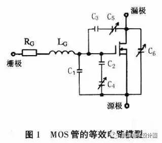
The relationship between MOS transistor input capacitor (Ciss), jumper capacitor (Crss), output capacitor (Coss), gate-source capacitance, gate-drain capacitance, and drain-source capacitance is as follows:

03
MOS tube opening process
The switch mode circuit of the switch tube is shown in Figure 2. The diode can be external or inherent to the MOS tube. The diode voltage and current waveform when the switch is turned on are shown in Figure 3.
In the phase 1 of Figure 3, the switching transistor is turned off, the switching current is zero, and the diode current and the inductor current are equal;
When the switch is turned on in phase 2, the switching current rises and the diode current drops. The slope of the rise of the switch current is the same as the absolute value of the slope of the diode current drop, with the opposite sign;
In phase 3, the switching current continues to rise, the diode current continues to drop, and the diode current sign changes from positive to negative;
In phase 4, the diodes decrease from the negative reverse maximum current IRRM, and their absolute slopes are equal; in phase 5, the switch is fully turned on, the diode's reverse recovery is complete, and the switch current is equal to the inductor current.
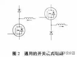
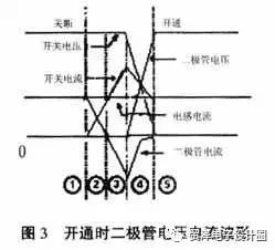
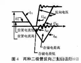
Figure 4 shows two diode current and voltage waveforms for storing high or low charge. It can be seen from the figure that when the stored charge is small, the slope of the reverse voltage is large and harmful vibration is generated. The low pre-current draws less charge, which is the worst condition at no load or light load. Therefore, when designing the optimized driver circuit, the case where the pre-current is low should be considered, that is, the case of no-load or light-load, so that the vibration generated by the diode should be within an acceptable range.
04
Relationship between gate charge QG and driving effect
The gate charge QG is the gate charge required to raise the gate voltage from 0 to 10 V, which can be expressed as the product of the drive current value and the turn-on time or the product of the gate capacitance value and the gate voltage. Most of the MOS transistors now have a gate charge QG value ranging from tens of nanocoulombs to one or two hundred nanocoulombs.
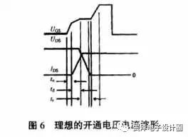
The gate charge QG contains two parts: the gate-to-source charge QGS; the gate-to-drain charge QGD—the “Miller†charge. QGS is the charge required to raise the gate voltage from 0 to the threshold (about 3V); QGD is the charge required to overcome the "Miller" effect when the drain voltage drops, which exists in the second segment where the UGS curve is relatively flat (eg As shown in Fig. 5, at this time, the gate voltage does not change, the gate charge accumulates, and the drain voltage agglomerates, that is, the peak current limit needs to be driven at this time, which is completed by the internal chip or by an external resistor. The actual QG can also be slightly larger to reduce the equivalent RON, but it is too big or too beneficial, so the driving voltage of 10V to 12V is reasonable. This also includes an important fact: a high peak current is required to reduce MOS tube losses and switching time.
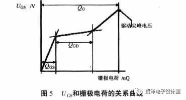
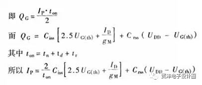
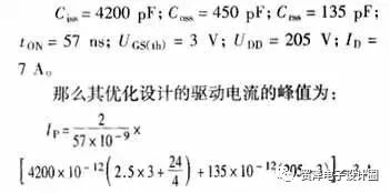
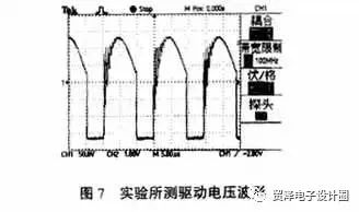
The important thing is that for the IC, the average capacitive load of the MOS transistor is not the input capacitance Ciss of the MOS transistor, but the equivalent input capacitance Ceff (Ceff=QG/UGS), that is, the whole 0. The drain current appears in the QGD phase of the QG waveform. The drain voltage is still high, the loss of the MOS transistor is the largest, and decreases with the decrease of UDS. Most of QGD is used to reduce the "Miller" effect of UDS from turn-off voltage to UGS(th). The equivalent load capacitance of the third segment of the QG waveform is: 05 Optimized gate drive design In most switching power application circuits, when the gate is driven, the drain current rises at a rate several times the drain voltage drop rate when the switch is turned on, which causes an increase in power loss. In order to solve the problem, the gate drive current can be increased, but increasing the gate drive rising slope will cause problems such as overshoot, oscillation, and EMI. Optimizing the gate drive design, it is precisely in the contradictory requirements to find a balance point, and this balance point is the waveform of the rising speed of the drain current and the falling speed of the drain voltage when the switch is turned on. The ideal driving waveform As shown in Figure 6. The UGS waveform of Figure 6 includes such parts: The first segment of UGS is fast rising to the threshold voltage; the second segment of UGS is a slower rising speed to slow down the rising speed of the drain current, but UGS must also meet the required drain current value; UGS fourth The fast rise of the segment causes the drain voltage to drop rapidly; the fifth segment of UGS is charged to the last value. Of course, it is very difficult to get the exact same drive waveform, but you can get a rough drive current waveform with a rise time equal to the ideal drain voltage fall time or drain current rise time, and have enough spikes to Large equivalent capacitance during the charge switch. The calculation of the gate peak current IP is such that the charge must fully satisfy the parasitic capacitance of the switching period. 06 Applications In the 48V50A circuit designed by the author, a two-transistor forward converter circuit is adopted, and the switch tube adopts IXFH24N50, and its parameters are: According to the above, the ideal waveform of the driving voltage and current should not be a straight line, but should be a waveform as shown in FIG. 6. The experimental waveform is shown in Figure 7. 07 in conclusion This paper introduces in detail the circuit model, switching process, input and output capacitance, equivalent capacitance, charge storage, etc. of the MOS tube, and the optimization design example of the driving waveform based on the influence of these parameters on the driving waveform. A good practical result has been achieved. In addition to its inherent Tr, Tf, there is an important parameter affecting the switching speed of the MOSFET: Qg (gate total static charge capacity). This parameter together with the output internal resistance of the gate drive circuit constitutes a time parameter, affecting MOSFET performance (the gate drive circuit of your motherboard's MOSFET is integrated in the IRU3055 PWM control chip); r6 @0 k" S/ l3 }4 u, r/ W The Tr and Tf values ​​given by the manufacturer are measured under the condition that the gate drive internal resistance is negligible, which is different in practical applications, especially the gate drive integrated circuit in the PWM chip, from PWM. The width and length of the wiring to the gate of the MOSFET will have a profound impact on the performance of the MOSFET. If the internal resistance of the PWM output is not low, and the Qg of the MOS transistor is large, then no matter how good the Tr and Tf are, it may be Significantly increase the time of ascent and descent I think that in the BUCK synchronous converter, the Qg of the high-side MOS transistor is more important than other parameters such as RDS. In addition, the matching of the gate drive internal resistance and Qg is also important, to some extent, the high side is determined by its charging time. MOSFET switching speed and loss.. See which angle to look at The charge is slowed down, indicating a large time constant. The time constant is the product of Ciss and Rgs. The large insulation resistance of the gate and source indicates that the manufacturing process is well controlled, and the surface impurities of the material, the chip and the package are less, and the leakage is less. The time constant is large, and the gate-source equivalent input capacitance is also large. The gate-equivalent equivalent input capacitance is proportional to the die size and is related to the die design. Generally, the die size is large, Ron (on-resistance) is small, and transconductance (gain) is large. Large gate-to-source equivalent capacitance increases switching time, reduces switching performance, reduces operating speed, and increases power loss. Ciss is proportional to the charge injection rate and may be related to the applied voltage and has nonlinearities. All of the above are comparisons under the same conditions. From the application point of view, at the same price, most designs want to use three devices with equivalent capacitors (including Ciss). Ciss=Cgd+Cgs, there is also a sequence of charge and discharge times, first Cgs is full, then Cgd. Aluminum Alloy Creative Notebook Stand Shenzhen ChengRong Technology Co.,Ltd. , https://www.dglaptopstandsupplier.com
