1 Introduction
The so-called current detection is used to detect the current passing through a component or a wire. Generally, a current signal is converted into a voltage signal by a transformer, a shunt, etc., and then processed and amplified for later circuit protection and detection. . Currently, many different current sensing technologies have been published or implemented. The commonly used DC current detection method is mainly through series resistance or based on the Hall effect principle. Under normal circumstances, the measured current signal is large, and the influence of series resistance on the input current signal is negligible, but with the development of science and technology The detected signal is gradually decreasing. If the series resistance is directly connected in the system circuit, it will affect the operation of the previous stage circuit, resulting in a change in the magnitude of the measured current signal. At this time, the influence can no longer be ignored.
In order to detect the small current signal and simultaneously reduce the input current signal to meet the requirements of the subsequent processing circuit, this paper presents two different methods commonly used in the traditional current detection circuit - resistance detection and current The detection circuit of the transformer detection is different from the circuit using the passive components such as resistors, capacitors and inductors as the main structure, and a current detection circuit composed of the MOS tube as the main structure is designed. It can overcome the problem of large change of the input current signal due to the large influence on the source current while realizing the current scaling.
2. Current detection circuit principle and design optimization 2.1 Design requirementsThe design of this paper relies on the automotive electronics national project service design platform. The current detection circuit required in the project mainly requires the reduction of the large current signal, and finally the smaller current signal output, in order to provide the required current value for the subsequent circuit module. At the same time, it is required to ensure that the input current value cannot be changed while obtaining a small output current. The design requires a target that achieves a 3600-fold reduction in output current compared to the input current, while requiring better linearity.
2.2 Structural designThe current detection circuit designed in this paper is mainly to reduce the input current so as to carry out other related operations on the current, such as overcurrent protection. It should be noted that the input current cannot be changed at the same time as the output current is obtained, or it has a large influence on it, so that the form of the resistor divider cannot be directly used. It is also expected that the accuracy of the current variation of the circuit can reach a reasonable range and have a stable output current. However, the uncertainty of the resistance is large in practical applications. The stability of the sheet resistance is not very good due to temperature, process, etc., and the fluctuation is large, which may cause the resistance value obtained after the final flow sheet to have a large deviation from the original design. Circuit performance. These two points are the key issues that need to be solved in the circuit design, and also the difficulty in designing.
In general, a key feature of a current mirror is that it accurately replicates current without being affected by process and temperature, and this structural characteristic itself determines that it has little effect on the input current. Considering the above design requirements and the circuit structure of the front-end circuit output, it is finally determined that the current mirror structure is used to realize the design.
In the current mirror configuration, the ratio of Iout to IREF (standard current, here the input current) is determined by the ratio of the device dimensions, which can be controlled within a reasonable accuracy range. It should be noted that all transistors in the current mirror typically use the same gate length to reduce errors due to edge-diffusion (LD) of the source and drain regions. Moreover, the threshold voltage of the short trench device has a certain dependence on the channel length. Therefore, the ratio of current values ​​can only be achieved by adjusting the width of the transistor. In addition, the adjustment of the device width is actually achieved by connecting a plurality of cell transistors in parallel, rather than simply designing to change the width of one device. Taking into account the layout and the impact of the process on the performance of the circuit, the transistor needs to adopt a symmetrical structure as much as possible. The final determined circuit structure is shown in Figure 1.
 Figure 1 Current detection circuit structure
According to the circuit structure, the circuit can be directly calculated to achieve a current reduction of 3600 times. The final determination of the size of each transistor in the circuit is obtained by comparing the simulation results of different device size circuits.
3. Optimization and simulationFirst, the selection of the transistor gate length is determined. According to the characteristics of the current mirror structure, all transistors in the current mirror usually use the same gate length. At the time of design, it is also necessary to consider the requirements of the process used in the final flow. This process uses a 0.5 μm process, so the L value should not be too small, otherwise the performance of the circuit will have a great dependence on process accuracy. By analyzing the circuit simulation results of different lengths (as shown in Figure 2), it can be known that the linearity of the circuit is optimal when L=1 μm, which can well meet the reasonable accuracy requirements.
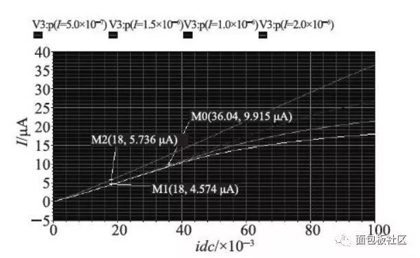 Figure 2 MOS tube L value impact on circuit performance simulation
Considering various factors in a comprehensive way, when selecting the gate length of the MOS tube, it is finally determined that L=1 μm is the optimal scheme for the circuit construction. This also shows that the current mirror structure should be used to change the ratio of the width of the MOS tube to adjust the current.
Next, the determination of the transistor width will be discussed. The ratio of the width of the transistor directly determines the multiple of the current reduction of the current. Figure 3 is a simulation result of the transistor width taking 2~8 μm in turn.
It should be noted that when the width is large, the area occupied by the entire transistor will also increase significantly. In addition, the number of NMOS and PMOS transistors will also have a certain impact on circuit performance. Therefore, considering the needs of the circuit variation multiple, the accuracy requirements, and the layout area, the circuit structure given in Figure 1 is finally determined.
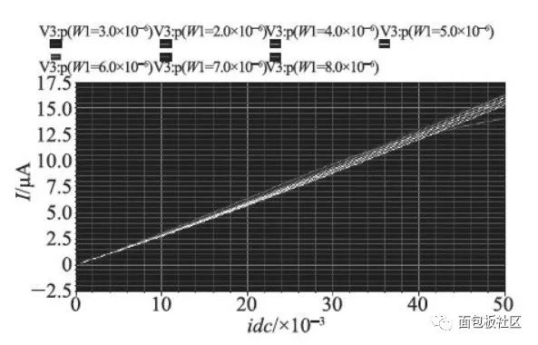 Figure 3 Circuit performance simulation at different widths
4. Performance simulation and test results
4.1 Simulation resultsFirst, the output characteristics of the circuit are simulated. Load R1 with different resistance values ​​for the circuit, perform simulation test separately, observe the change of output characteristics, and the result is shown in Figure 4.
 Figure 4 Circuit performance simulation under different R1
It can be clearly seen from Figure 4 that when the circuit is loaded with different loads, the output of the circuit almost completely coincides, indicating that the load has no effect on the output. This result is a good illustration of the circuit structure has a very stable output characteristics, the circuit design can achieve a stable output design goals.
At the same time, it can be clearly seen from the two special points marked in Fig. 4 that the circuit structure finally realizes that the circuit current variation value is smaller than the theoretical value. The post-simulation structure of the circuit is very different from the pre-simulation result. Therefore, it can be said that the whole circuit can basically meet the linearity requirement and realize the circuit function under the premise of considering the process volatility.
4.2 Test resultsFig. 5 is a layout of the current detecting circuit when the film is finally processed. It can be seen that the entire circuit core is almost entirely composed of MOS tubes. Table 1 is the final result of testing the circuit in the chip. Due to test conditions, only some discontinuous current value points can be given as inputs. In the test, we measured a number of circuits, and the test results of most of the circuits are relatively close. Table 1 gives two sets of typical data.
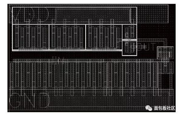 Figure 5 layout of the current detection circuit
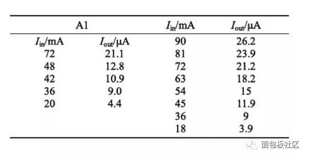 Table l More typical two sets of test data
Through the test results, it can be seen that the entire circuit basically realizes the functional requirements of the design, and the function of reducing the current is completed. The magnification of the two sets of data results given in the table is not much different from the simulation results, which basically meets the design requirements. In the actual test, a set of data with large deviations appeared. The results of these test data were selected by using different 5×5 chips. This shows that due to process problems, there are certain performance deviations in the circuits at different locations, and the performance of individual circuits may not be ideal. However, this is a process variation within the design considerations, and it also indicates that the process is unstable.
In order to see the circuit current variation characteristics more intuitively, we draw the second set of data in Table 1 into a curve. The result is shown in Figure 6. Through the data sorting calculation, it can be known that the test result differs from the simulation result by about 1 μA, and when the input current value is larger, the deviation is slightly reduced, and the accuracy of the obtained output current is higher. The entire circuit can better achieve the circuit reduction function, and can achieve the 3600 times reduction value of the design requirements. At the same time, the linearity of the test results is within a reasonable range.
Overall, the final test results are acceptable, which means that the circuit can perform its functions better.
5. Data extractionWith the rapid development of the information industry, the use of IP cores has received increasing attention from the industry. According to Dataquest, the IP core has become an industry. The design of the circuit is to realize the design of the IP core module. Therefore, after completing the basic circuit design, the flow film, and the test work, the related data is also packaged to facilitate the multiplexing of the IP core. Data processing includes the extraction of LEF files for circuits and the writing of logic functions (Verilog-A code).
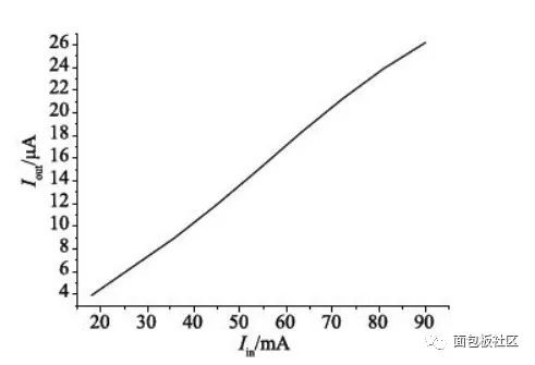 Figure 6 current detection circuit test results
The LEF file was generated using Cadence's data extraction tool Abstracts Generating for IP core data extraction. Abstract mainly extracts the various devices and pin information of the circuit according to three basic data - TECH.lef, each circuit layout information (GDSII) and MAP to be extracted, and obtains the lef file abstract.lef.
The logic function is written in a high-level analog circuit hardware description language Verilog-A code. Figure 7 shows that the simulation results of the code are basically consistent with the simulation of the above circuit structure, indicating that the code written can normally implement the current detection function. This completes the basic work of writing the logic function of the circuit and data extraction, and provides data support for the multiplexing of the IP core.
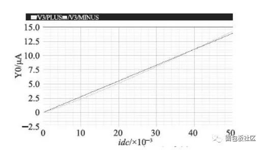 Figure 7 VerilogA code simulation results
The current detection circuit plays an important role in current control and protection. The current detection circuit in this paper uses active devices to complete the circuit design, and basically realizes the function of current detection. Structural optimization is performed by considering performance requirements and process constraints in the circuit design process. Subsequent registration function overcurrent protection circuits can also achieve functional requirements.
T Copper Tube Terminals,Non-Insulated Pin-Shaped Naked Terminal,Copper Cable Lugs Terminals,Insulated Fork Cable Spade Terminal
Taixing Longyi Terminals Co.,Ltd. , https://www.lycopperlugs.com