introduction
Nuclear energy spectrum amplifiers are an important part of the energy spectrum measurement system, and their performance directly affects the resolution of the entire spectrum measurement system. This paper improves the shortcomings of traditional nuclear spectrum signal amplifiers. Design and develop a general-purpose, multi-programmable nuclear energy spectrum signal amplifier, which can be applied to X-ray fluorescence spectrometers, gamma spectrometers and other nuclear energy spectrum measuring instruments, and has universality. The amplifier, such as further fusion signal acquisition (A/D conversion) technology and digital signal processing (DSP) technology, can form a fully functional nuclear energy spectrum signal processing system.
1 circuit basic composition
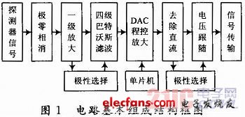
The circuit mainly includes three parts: filter shaping, program-controlled amplification, and baseline elimination. The filter shaping circuit includes a zero-zero cancellation, a four-stage Butterworth filter circuit, and a polarity selection circuit; the program-controlled amplifier circuit includes a first-order 20-times amplification and a 12-bit DAC program-controlled amplification circuit; the baseline cancellation circuit includes a DC removal circuit, and an inversion Circuit and voltage follower circuit, block diagram shown in Figure 1.
2 unit circuit principle analysis
2.1 Extreme zero cancellation
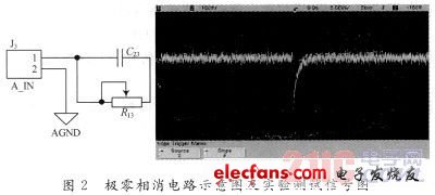
The signal input terminal is connected to the zero-zero cancellation circuit to eliminate the downstroke caused by the differentiation of the probe signal, so that the pulse monotonously returns to the baseline, which improves the effect of the count rate overload and the pulse amplitude superposition, and is suitable for high resolution. And a high count rate spectrometer system. Figure 2 shows the design circuit and experimental test signal diagram.
2.2 Filter shaping
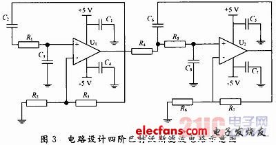
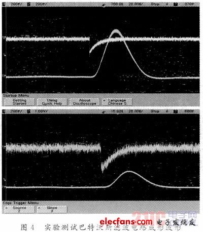
The circuit is cascaded into four fourth-order Butterworth filter circuits using two second-order Butterworth filter circuits. A second-order low-pass Butterworth filter circuit designed with an operational amplifier is directly obtained by frequency domain analysis:
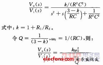
Where: k is equivalent to the voltage amplification factor of the non-inverting amplifier, called the passband gain of the filter; Q is the quality factor; ω0 is the characteristic angular frequency. Figure 3 is a schematic diagram of the circuit design of the filter forming part, and Figure 4 is the experimental test result.
Hinger,hinger for game,slot game hinger
Guangzhou Ruihong Electronic Technology CO.,Ltd , https://www.callegame.com