This paper will explain how the SAR ADC operates using a binary search algorithm to converge on the input signal. It also provides an explanation for the heart of the SAR ADC, the capacitive DAC and also the high-speed comparator. Finally, the article will contrast the SAR architecture against pipeline, flash ADCs.
Successive-approximation-register (SAR) analog-to-digital converters (ADCs) are frequently the architecture of choice for medium-to-high-resolution applications with sample rates under 5 megasamples per second (Msps). SAR ADCs most commonly range in resolution from 8 to 16 bits and provide low power consumption as well as a small form factor. This combination makes them ideal for a wide variety of applications, such as portable / battery-powered instruments, pen digitizers, industrial controls, and data / signal acquisition.
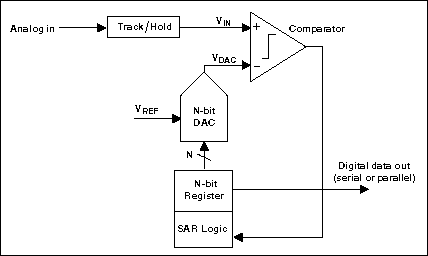
As the name implies, the SAR ADC basically implements a binary search algorithm. Therefore, while the internal circuitry may be running at several megahertz (MHz), the ADC sample rate is a fraction of that number due to the successive-approximation algorithm. SAR ADC ArchitectureAlthough there are many variations in the implementation of a SAR ADC, the basic architecture is quite simple (see Figure 1). The analog input voltage (VIN) is held on a track / hold. To implement the binary search algorithm, the N -bit register is first set to midscale (that is, 100 ... .00, where the MSB is set to '1'). This forces the DAC output (VDAC) to be VREF / 2, where VREF is the reference voltage provided to the ADC. A comparison is then performed to determine if VIN is less than or greater than VDAC. If VIN is greater than VDAC, the comparator output is a logic high or '1' and the MSB of the N-bit register remains at '1'. Conversely, if VIN is less than VDAC, the comparator output is a logic low and the MS B of the register is cleared to logic '0'. The SAR control logic then moves to the next bit down, forces that bit high, and does another comparison. The sequence continues all the way down to the LSB. Once this is done, the conversion is complete, and the N-bit digital word is available in the register.

Figure 1. Simplified N-bit SAR ADC architecture.
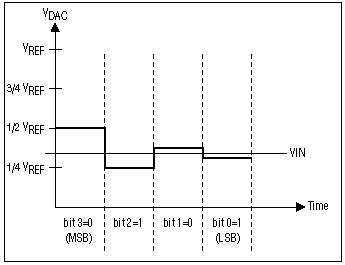
Figure 2 shows an example of a 4-bit conversion. The y-axis (and the bold line in the figure) represents the DAC output voltage. In the example, the first comparison shows that VIN <VDAC. Thus, bit 3 is set to '0'. The DAC is then set to 01002 and the second comparison is performed. As VIN> VDAC, bit 2 remains at '1'. The DAC is then set to 01102, and the third comparison is performed. Bit 1 is set to '0', and the DAC is then set to 01012 for the final comparison. Finally, bit 0 remains at '1' because VIN> VDAC.

Figure 2. SAR operation (4-bit ADC example).
Notice that four comparison periods are required for a 4-bit ADC. Generally speaking, an N-bit SAR ADC will require N comparison periods and will not be ready for the next conversion until the current one is complete. This explains why these types of ADCs are power- and space-efficient, yet are rarely seen in speed-and-resolution combinations beyond a few Msps at 14 to 16 bits. Some of the smallest ADCs available on the market are based on the SAR architecture. The MAX1115-MAX1118 series of 8-bit ADCs as well as their higher-resolution counterparts, the MAX1086 and the MAX1286 (10 and 12 bits, respectively), fit in tiny SOT23 packages measuring 3mm by 3mm.
One other feature of SAR ADCs is that power dissipation scales with the sample rate, unlike flash or pipelined ADCs, which usually have constant power dissipation versus sample rate. This is especially useful in low-power applications or applications where the data acquisition is not continuous (for example, PDA digitizers). In-Depth SAR AnalysisThe two critical components are the comparator and the DAC. As we shall see later, the track / hold shown in Figure 1 can be embedded in the DAC and may not be an explicit circuit .
A SAR ADC's speed is limited by: The settling time of the DAC, which must settle to within the resolution of the overall converter, for example, 1 / 2LSB The comparator, which must resolve small differences in VIN and VDAC within the specified time The logic overhead DACThe maximum settling time of the DAC is usually determined by the MSB settling. This is simply because the MSB transition represents the largest excursion of the DAC output. In addition, the linearity of the overall ADC is limited by the linearity of the DAC Therefore, SAR ADCs with more than 12 bits of resolution will often require some form of trimming or calibration to achieve the necessary linearity. This is due to the inherent component-matching limitations. Although it is somewhat process-and-design-dependent, component matching limits the linearity to about 12 bits in practical DAC designs. Many SAR ADCs use a capacitive DAC that provides an inherent track / hold function. Capacitive DACs employ the principle of cha rge redistribution to generate an analog output voltage. Because these types of DACs are prevalent in SAR ADCs, it is beneficial to discuss their operation.
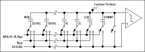
A capacitive DAC consists of an array of N capacitors with binary weighted values ​​plus one "dummy LSB" capacitor. Figure 3 shows an example of a 16-bit capacitive DAC connected to a comparator. During the acquisition phase, the array's common terminal (the terminal at which all the capacitors share a connection, see Figure 3) is connected to ground and all free terminals are connected to the input signal (Analog In or VIN). After acquisition, the common terminal is disconnected from ground and the free terminals are disconnected from VIN, effectively trapping a charge proportional to the input voltage on the capacitor array. The free terminals of all the capacitors are then connected to ground, driving the common terminal negative to a voltage equal to -VIN.

Figure 3. Capacitive DAC (16-bit example).
As the first step in the binary search algorithm, the free terminal of the MSB capacitor is disconnected from ground and connected to VREF, driving the common terminal in the positive direction by an amount equal to 1 / 2VREF. For example, if VIN is equal to 3 / 4VREF, connecting the MSB capacitor to VREF and the rest of the capacitors to ground will drive the common terminal to (-3 / 4VREF + 1 / 2VREF) =-1 / 4VREF. When this voltage is compared to ground, the comparator output yields a logic '1', implying that the MSB is greater than 1 / 2VREF. Conversely, if VIN is equal to 1 / 4VREF, the common terminal voltage is (-1 / 4VREF + 1 / 2VREF) = + 1 / 4VREF, and the comparator output is a logic '0'. Following this, the next-largest capacitor is disconnected from ground and connected to VREF, and the comparator determines the next bit. This continues until all bits have been determined. DAC CalibrationIn an ideal DAC, each of the capacitors associated with the data bits would be exactly twice the value o f the next-smaller capacitor. In high-resolution ADCs (for example, 16-bit), this results in a range of values ​​too wide to be realized in an economically feasible size. The 16-bit SAR ADCs such as the MAX195 utilize a capacitor array that actually consists of two arrays that are capacitively coupled to reduce the LSB array's effective value. The capacitors in the MSB array are production-trimmed to reduce errors. Small variations in the LSB capacitors contribute insignificant errors to the 16-bit result Unfortunately, trimming alone does not yield 16-bit performance or compensate for changes in performance due to changes in temperature, supply voltage, and other parameters. For this reason, the MAX195 includes a calibration DAC for each capacitor in the MSB array. These DACs are capacitively coupled to the main DAC output and offset the main DAC's output according to the value on their digital inputs.
During calibration, the correct digital code to compensate for the error in each MSB capacitor is determined and stored. Recovered, the stored code is provided to the appropriate-calibration DAC whenever the corresponding bit in the main DAC is high, compensating for errors in the associated capacitor. Calibration is usually initiated by the user or done automatically on power-up. To reduce the effects of noise, each calibration experiment is performed many times (about 14,000 clock cycles in the MAX195), and the results are averaged. Calibration is best performed when the power-supply voltages are stable, and high-resolution ADCs should be recalibrated any time there is a significant change in supply voltages, temperature, reference voltage, or clock characteristics, because these parameters affect the DC offset. If linearity is the only concern, much larger changes in these parameters can be tolerated. Because the calibration data is stored digitally, there is no need to perform fre quent conversions to maintain accuracy. ComparatorThe requirements of the comparator are speed and accuracy. Comparator offset does not affect overall linearity as it appears as an offset in the overall transfer characteristic. In addition, offset-cancellation techniques are usually applied to reduce the comparator offset . Noise, however, is a concern, and the comparator is usually designed to have input-referred noise less than 1LSB. Additionally, the comparator needs to resolve voltages within the accuracy of the overall system; in other words, the comparator needs to be as accurate as the overall system. SAR ADCs versus Other ADC Architectures Versus PipelinedA pipelined ADC employs a parallel structure in which each stage works on one to a few bits (of successive samples) concurrently. The inherent parallelism increases throughput, but at the expense of power consumption and latency. Latency in this case is defined as the difference between the time an analog sample is acquired by the ADC and the time when the digital data is available at the output. For instance, a five-stage pipelined ADC will have at least five clock cycles of latency, whereas a SAR has only one clock cycle of latency. Note that the latency definition applies only to the throughput of the ADC, not the internal clock of a SAR, which runs at many times the frequency of the throughput. Pipelined ADCs frequently have digital error correction logic to reduce the accuracy requirement of the flash ADCs (that is, comparators ) in each pipeline stage. On the other hand, a SAR ADC requires the comparator to be as accurate as the overall system. A pipelined ADC generally takes up significantly more silicon area than an equivalent SAR. Like a SAR, a pipelined ADC with more than 12 bits of accuracy usually requires some form of trimming or calibration. Versus FlashA flash ADC is made up of a large bank of comparators, each consisting of wideband, low-gain preamp (s) followed by a latch. The preamps only hav e to provide gain but do not need to be linear or accurate; meaning, only the comparators' trip points have to be accurate. As a result, flash ADC is the fastest architecture available. The primary trade-off for speed is the significantly lower power consumption and the smaller form factor. Although extremely fast 8-bit flash ADCs (or their folding / interpolation variants) exist with sampling rates as high as 1.5GS / s (for example, the MAX104 / MAX106 / MAX108), it is much harder to find a 10-bit flash, while 12-bit (and above) flash ADCs are not commercially viable products. This is simply because in a flash the number of comparators goes up by a factor of 2 for every extra bit of resolution, and, at the same time, each comparator has to be twice as accurate. In a SAR ADC, however, the increased resolution requires more accurate components, yet the complexity does not increase exponentially. Of course, SAR ADCs are not capable of speeds anywhere close to those of flash ADCs. Versus Sigma-De lta ConverterTraditional oversampling / sigma-delta-type converters commonly used in digital audio applications have limited bandwidths of about 22kHz. Recently, some high-bandwidth sigma-delta-type converters have reached bandwidths of 1MHz to 2MHz with 12 to 16 bits of resolution. These are usually very-high-order sigma-delta modulators (for example, 4th-order or higher) incorporating a multi-bit ADC and multi-bit feedback DAC. Sigma-delta converters have the innate advantage of requiring no special trimming or calibration , even to attain 16 to 18 bits of resolution. They also do not require anti-alias filters with steep roll-offs at the analog inputs, because the sampling rate is much higher than the effective bandwidth; the backend digital filters take care of this . The oversampling nature of the sigma-delta converter may also tend to "average out" any system noise at the analog inputs. However, sigma-delta converters trade speed for resolution. The need to sample many times (at leas t 16 times and often more) to produce one final sample dictates that the internal analog components in the sigma-delta modulator operate much faster than the final data rate. The digital decimation filter is also a challenge to design and consumes a lot of silicon area . The fastest high-resolution sigma-delta converters are not expected to have significantly higher bandwidth than a few MHz in the near future. ConclusionIn summary, the primary advantages of SAR ADCs are low power consumption, high resolution and accuracy, and a small form factor. Because of these benefits, SAR ADCs can often be integrated with other larger functions. The main limitations of the SAR architecture are the lower sampling rates and the requirements for the building blocks (such as the DAC and the comparator) to be as accurate as the overall system. References Maxim Integrated Products; MAX195 data sheet, Rev 1, 12/1997.
Razavi, Behzad; Principles of Data Conversion System Design; IEEE Press, 1995.
Van De Plassche, Rudy; Integrated Analog-to-Digital and Digital-to-Analog Converters; Kluwer Academic Publishers, 1994.
Maxim Integrated Products; Understanding Pipelined ADCs.
All In One Gaming PC is the best choice when you are looking higher level desktop type computer for heaver tasks, like engineering or architecture drawings, designing, 3D max, video or music editing, etc. What we do is Custom All In One Gaming PC, you can see Colorful All In One Gaming PC at this store, but the most welcome is white and black. Sometimes, clients may ask which is the Best All In One Gaming PC? 23.8 inch i7 or i5 11th generation All In One Gaming Desktop PC should beat it. Cause this configuration can finish more than 80% task for heavier jobs. Business All In One Computer and All In One Desktop Touch Screen is other two popular series. Multiple screens, cpu, storage optional. Except All In One PC, there are Education Laptop, Gaming Laptop, i7 16gb ram 4gb graphics laptop, Mini PC , all in one, etc.
Any other unique requirements, Just feel free to contact us and share your ideas, thus more matched details sended in 1-2working days. Will try our best to support you.
Of course, any we can do in China, also willing to do it for you.
All In One Gaming PC,Best All In One Gaming Pc,Colorful All In One Gaming Pc,Custom All In One Gaming Pc,All In One Gaming Desktop Pc
Henan Shuyi Electronics Co., Ltd. , https://www.shuyihost.com