In general isolated power supplies, optocoupler isolation feedback is a simple, low-cost way. However, for the various coupling methods and their differences in optocoupler feedback, no more in-depth studies have been seen yet. Moreover, in many cases, due to the lack of understanding of the optocoupler working principle, the optocoupler connection is confusing, which often results in the circuit not working properly. This study will analyze the optocoupler working principle in detail, and compare and study several typical connections of optocoupler feedback.
1, several common connection methods and their working principle
Photocouplers commonly used for feedback include TLP521 and PC817. Here takes the TLP521 as an example to introduce the characteristics of this type of optocoupler. The primary side of the TLP521 is equivalent to a light emitting diode. The greater the primary current If is, the stronger the light intensity is, and the larger the current Ic of the secondary transistor is. The ratio of the secondary-side transistor current Ic to the primary-side diode current If is referred to as the current-amplification coefficient of the optocoupler. The coefficient changes with temperature and is greatly affected by temperature. The optocoupler used for feedback is to use “the change of the primary current will cause the secondary current to change†to realize feedback. Therefore, in the occasion where the ambient temperature changes violently, the temperature drift of the amplification factor is relatively large, and it should be avoided by the optocoupler. Feedback.
In addition, the use of such optocouplers must pay attention to the design of peripheral parameters to make it work in a relatively wide linear band, otherwise the sensitivity of the circuit to the operating parameters is too strong, is not conducive to the stable operation of the circuit. Usually choose TL431 to combine with TLP521 for feedback. At this time, the working principle of the TL431 is equivalent to a voltage error amplifier with an internal reference of 2.5V. Therefore, the compensation network must be connected between the 1st pin and the 3rd pin. The first type of common optocoupler feedback is shown in Figure 1. In the figure, Vo is the output voltage and Vd is the supply voltage of the chip. The com signal is connected to the error amplifier output pin of the chip, or the internal voltage error amplifier of the PWM chip (such as the UC3525) is connected in the form of an in-phase amplifier. The com signal is connected to its corresponding non-inverting pin.
Note that the ground on the left is the output voltage ground, and the ground on the right is the chip supply voltage ground. The two are isolated by optocoupler. The working principle of the connection shown in Figure 1 is as follows: When the output voltage rises, the TL431's pin 1 (equivalent to the voltage error amplifier's inverting input) rises, and pin 3 (equivalent to the voltage error amplifier's output pin) voltage If the primary current If of the optocoupler TLP521 increases, the output current Ic at the other end of the optocoupler increases, the voltage drop at the resistor R4 increases, the voltage at the com pin decreases, the duty cycle decreases, and the output voltage decreases. Conversely, when the output voltage decreases, the regulation process is similar.
The common second connection is shown in Figure 2. Different from the first connection method, the 4th pin of the optocoupler is directly connected to the output end of the error amplifier of the chip, and the voltage error amplifier inside the chip must be connected so that the non-inverting potential is higher than the inverting potential. Form, a feature of the op amp - when the output current of the op amp is too large (exceeds the output current capability of the op amp), the output voltage of the op amp will drop, the greater the output current, the more the output voltage will drop. Therefore, using this method of connection, the two input pins of the error amplifier of the PWM chip must be connected to a fixed potential, and the potential of the same terminal should be higher than the potential of the opposite terminal, so that the initial output voltage of the error amplifier. High.
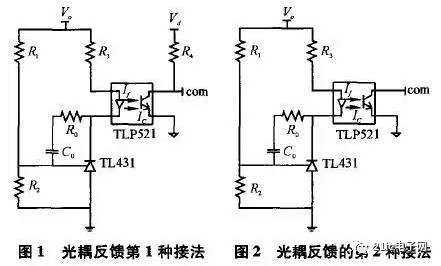
The working principle of the connection method shown in FIG. 2 is as follows: when the output voltage increases, the primary current If increases and the output current Ic increases. Since Ic has exceeded the current output capability of the voltage error amplifier, the com pin voltage drops, accounting for The space ratio decreases and the output voltage decreases; conversely, when the output voltage drops, the regulation process is similar.
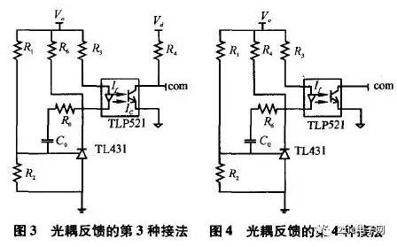
The common third connection is shown in Figure 3. Basically similar to Figure 1, except that in Figure 3 there is a resistor R6, the role of this resistor is to inject a current to the TL431, to avoid the TL431 due to the injection current is too small to work properly. In fact, if the resistance value R3 is properly selected, the resistor R6 can be omitted. The adjustment process is basically the same as the connection method in Figure 1.
The common fourth connection is shown in Figure 4. The connection method is similar to the second connection method except that a resistor R4 is connected between the com terminal and the optocoupler pin 4, and its function is the same as that of the R6 in the third connection method. The operating principle is basically the same as the connection method. 2.
2. Comparison of various connection methods
Prior to comparison, several characteristics of the actual optocoupler TLP521 need to be analyzed. The first is the Ic-Vce curve, as shown in Figure 5 and Figure 6.
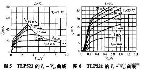
From Fig. 5 and Fig. 6, it can be seen that when the If is less than 5mA, slight changes in If will cause dramatic changes in Ic and Vce, and the output characteristics of the optocoupler will be flat. At this time, if the optocoupler is used as part of the power feedback network, the gain of its transfer function is very large. For the entire system, a very high gain can easily cause system instability. Therefore, it is not appropriate to set the static operating point of the optocoupler to a current If of less than 5 mA. It is appropriate to set it to 5 to 10 mA. In addition, the Ic-If curve of the optocoupler needs to be analyzed, as shown in Figure 7. As can be seen from Figure 7, when the current If is less than 10mA, Ic-If basically unchanged, and after the current If greater than 10mA, the optocouple began to saturate, Ic-If's value decreases with If increases. For a power supply system, if the gain of the loop is changed, it may cause instability, so it is not reasonable to set the static operating point to a point where If is too large (thereby output characteristics are easily saturated). It should be noted that the Ic-If curve changes with temperature, but the temperature change affects the Ic value at a certain fixed If value, basically no effect on the Ic-If ratio, the shape of the curve is still the same as Figure 7, As the temperature rises, the overall curve shifts downward. This characteristic can be seen from the Ic-Ta curve (as shown in Figure 8).
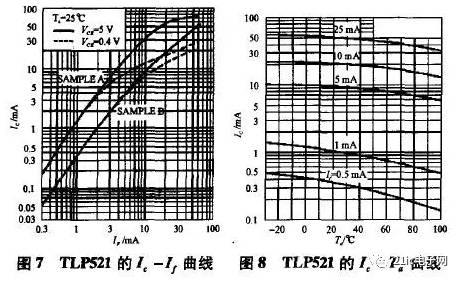
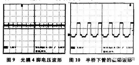
As can be seen from FIG. 8 , the Ic-Ta curves are substantially parallel to each other when If is greater than 5 mA. Based on the above analysis, the following is for different typical connections, comparing their characteristics and scope of application. This study uses the actual isolated half-bridge auxiliary power supply and flyback power supply as examples. In the first type of connection, the voltage received at the output of the voltage error amplifier is obtained after the external voltage is stepped down by the resistor R4 and is not affected by the current output capability of the voltage error amplifier. The operating point of the optocoupler can be optionally adjusted through its external resistance. According to the previous analysis, the static operating point value of the current If is approximately 10 mA, and the corresponding optocoupler operating temperature varies from 0 to 100° C., and the value is between 20 and 15 mA. The amplitude of the triangle wave of the general PWM chip does not exceed 3V. Therefore, the size of the resistor R4 is selected to be 670Ω, and at the same time, it is determined that the static operating point value of the TL431's 3 pin voltage is 12V, then the value of the resistor R3 can be selected to be 560Ω. The values ​​of the resistors R1 and R2 are easy to choose, here they are 27k and 4.7k. Resistor R5 and capacitor C1 are PI compensated, here taken as 3k and 10nF. In the experiment, the output load of the half-bridge auxiliary power supply was various control chips on the control board, plus the dead load of each of the multiple outputs, and the final actual power was about 30W. The actually measured optocoupler 4 pin voltage (this voltage is compared with the chip triangle wave to determine the driving duty cycle) waveform, as shown in Figure 9. The corresponding drive signal waveform is shown in Figure 10. The driving waveform of FIG. 10 has a negative voltage portion because the driving of the upper and lower tubes is wound on one driving magnetic ring. It can be seen that the duty cycle of the drive signal is relatively large, about 0.7.
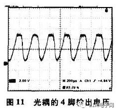
For the second type of connection, the voltage error amplifier inside the general chip has a maximum current output capability of about 3 mA. If the current value exceeds this value, the maximum voltage output by the error amplifier will drop. Therefore, in this connection method, if the steady-state duty ratio of the power supply is large, the current Ic is relatively small, and its value may be only slightly larger than 3 mA. Corresponding to FIG. 7, Ib is about 2 mA. It can be seen from Fig. 6 that when the Ib value is small, a small Ib change will cause Ic to change drastically, and the gain of the optocoupler will be very large, which will result in the closed loop network being less stable. If the power supply steady-state duty cycle is relatively small, the optocoupler 4 pin voltage is relatively small, corresponding to the output current of the voltage error amplifier is larger, that is, Ic is relatively large (far more than 3mA), the corresponding Ib is also relatively large, the same Corresponding to Fig. 6, when the Ib value is large, the corresponding optocoupler gain is relatively moderate, and the closed-loop network is relatively stable. Similarly, for the above half-bridge auxiliary power supply circuit, using connection 2 instead of connection 1, closed-loop instability, with an oscilloscope to observe the optocoupler 4-pin voltage waveform, there is significant oscillation. The optocoupler's 4-pin output voltage (corresponding to the UC3525's error amplifier output pin voltage) is shown in Figure 11 and noticeable oscillations can be found. This is due to the relatively large steady-state duty cycle of this half-bridge power supply. According to connection method 2, the optocoupler gain is large, and the system is unstable and oscillates.
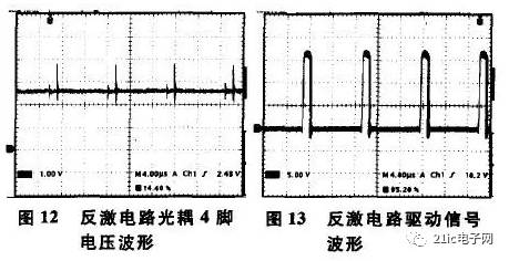
In fact, the second kind of connection is more common in the flyback circuit. This is because the flyback circuit is generally considered for efficiency. The circuit usually works in the discontinuous mode, and the driving duty ratio is relatively small, corresponding to the optocoupler current Ic. Large, with reference to the above analysis, it can be seen that the closed-loop loop is also easier to stabilize. The following is another experimental flyback circuit, working in discontinuous mode, actually measured its optocoupler 4-pin voltage waveform, as shown in Figure 12. The actual measured drive signal waveform, as shown in Figure 13, has a duty cycle of approximately 0.2.
Therefore, in the optocoupler feedback design, in addition to setting its peripheral parameters according to the characteristic parameters of the optocoupler, it should also be known that the selection of the feedback mode is also limited at different duty cycles. Feedback modes 1 and 3 are applicable to any duty cycle condition, while feedback modes 2 and 4 are more suitable for use where the duty cycle is relatively small.
3ã€Conclusion
This study lists four typical optocoupler feedback connections, analyzes the principles of optocoupler feedback and various limiting factors for various connections, and compares the differences in various connections. Through the actual half-bridge and flyback circuit tests, the limitations of the duty cycle of the circuit on the selection of the feedback mode are verified. Finally, the optocoupler feedback is summarized, which has certain reference value for the future optocoupler feedback design.
Iplay Vape - Manufacturers, Factory, Suppliers From China
We intention to see quality disfigurement within the creation and supply the ideal support to domestic and overseas buyers wholeheartedly for Iplay Vape, Vape Bar , Vape Pod System , Cbd Vape Disposable ,Cloud Vape.The principle of our company is to provide high-quality products, professional service, and honest communication. Welcome all friends to place trial order for creating a long-term business relationship.

IPALY Vape,IPALY Disposable E-Cigarette,IPALY Disposable Vape Pen,IPALY Disposable Device,IPALY 500Mah Vape Kit
TSVAPE Wholesale/OEM/ODM , https://www.tsecigarette.com