Frequently, when the RF counterparts ask about the design of microstrip lines, what type of microstrip is better? Or do ordinary microstrip lines and CPW/CPWG coplanar waveguide structures have those advantages and disadvantages? This problem seems simple, but there is little information to give a more positive answer, the following will be combined with Rogers's related literature, to answer this question.
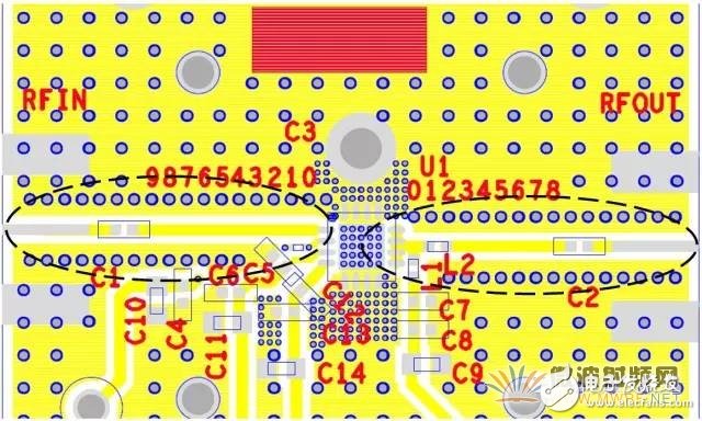
From the radio frequency to the millimeter wave band, coplanar waveguide (CPW) circuits are commonly used microstrip forms. The traditional coplanar waveguide is to form a conductor line on the surface of the PCB dielectric substrate, and the bottom layer is made into a planar GND layer. The circuit known as a grounded coplanar waveguide (CPW or CPWG) is an improved circuit for a conventional coplanar waveguide. The CPWG adds a ground plane to the underside of the CPW circuit structure and connects via the vias to the upper and lower ground planes.

Although both CPW and CPWG circuits have excellent isolation of adjacent channel signals, crosstalk in high-density circuits is reduced. However, compared to CPWs, CPWGs increase the amount of radiation at discontinuities due to the design of ground vias in the CPWG that can affect the impedance and increase losses. On the other hand, when the operating frequency is increased, the design of the CPWG ground hole can allow a larger dielectric material thickness than the microstrip circuit. Second, in high power circuit applications, the CPWG has better thermal performance than the CPW, and the increased ground plane also improves the mechanical stability of the circuit. Finally, when operating at microwave and millimeter wave frequencies, the CPWG has less surface wave leakage and radiation loss for the microstrip line and CPWG of the same circuit material.

In the millimeter-wave and lower frequency bands, CPW and CPWG have relatively simple production processes and good circuit performance stability. Most of the energy of the electromagnetic wave propagating through the transmission line, especially the CPWG, remains inside the PCB dielectric material. Compared with microstrip circuits, although both CPW and CPWG have higher conductor losses, the loss characteristics of CPW and CPWG circuits are linear with frequency. In microstrip circuits, especially at higher frequencies, losses (associated with radiation losses) will change with frequency. In addition, CPW and CPWG losses can be reduced by properly designing via locations and circuit dimensions.

In high-frequency bands such as millimeter waves, the size of the circuit becomes smaller and smaller, and the size of many key components in the circuit will be close to the wavelength of the signal transmitted by the circuit. For microstrip and stripline, the reflection loss and radiation loss will increase with the increase of frequency, and choosing the right circuit design becomes more critical. If designed properly, CPW, especially CPWG circuits, can achieve good performance at high frequencies and can often be combined with microstrip lines. In many high-frequency design examples, the CPWG serves as a high-performance interface at the microstrip transmission line interface.
CPW is to make conductors on the top layer of the dielectric substrate and make ground planes on both sides of the conductor to present a ground-signal-ground (GSG) layout. The ground plane and the signal line of the CPW are coplanar, and the impedance is controlled by adjusting the width of the signal line and the distance between the signal line and the ground. When the width of the signal line is tapered to the connector pin, the CPW impedance value can be kept constant.
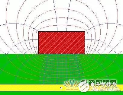
The CPWG adds a ground plane to the bottom of the dielectric layer and connects the top and bottom ground planes through vias. In the CPW electromagnetic energy is mainly concentrated in the dielectric layer. For CPW and CPWG, when the thickness of the dielectric substrate is more than twice the conductor width, electromagnetic energy leakage into the air can be effectively suppressed. When more than 2 times, the characteristic impedance is basically determined by the width of the center wire and the spacing between the wire and the ground plane. The CPW characteristic impedance is usually in the range of 20-250 Ω, while the characteristic values ​​of the microstrip line and the stripline are typically 20-120 Ω and 35-250 Ω, respectively.
Coupling in CPW and CPWGAs with any circuit technology, CPW and CPWG have their own advantages and disadvantages. For different application needs, including digital circuits and analog circuits, the advantages and disadvantages must be comprehensively weighed. The odd-mode and even-mode currents generated by the CPW and CPWG top-level ground lines can cause coupling of various modes of the circuit. When the frequency is increased, the closer spacing distances between the CPW and the CPGS GSG structure are likely to form strong coupling, to obtain better spurious mode suppression capability, and radiation loss is also lower. Increasing the spacing between signal lines and ground or increasing the signal line width (low conductor loss and insertion loss) can effectively reduce losses. When the distance between the signal line and the ground is appropriately increased, ie, loose coupling is achieved, the conductor loss and insertion loss of the circuit can be reduced. But the price is to bring more serious radiation loss and spurious distortion. Therefore, for the CPW and CPWG, the appropriate coupling strength is selected to both benefit low loss and effectively suppress the parasitic mode.
In general, the thinner the circuit, the better it is to reduce the radiation loss. For millimeter-wave circuits operating at 30 GHz or higher, radiation loss is an important part of the overall circuit loss. The radiation loss is largely related to the Dk value (dielectric constant) of the PCB material. The higher the Dk value of the circuit material, the smaller the radiation loss of the circuit, but the higher Dk value will bring more conductor loss. Because when the Dk value increases, the signal line width becomes narrow in order to maintain the characteristic impedance unchanged. Therefore, the conductor loss will increase.

Copper surface roughness in PCB circuits affects electric fields and currents. The effective dielectric constant increases as the copper surface roughness increases. In addition, copper surface roughness can affect the insertion loss of the circuit. Usually, the influence of CPWG is smaller than that of the microstrip line. Because in the CPWG circuit, the electric field and current are concentrated inside the GSG region on the PCB. In the microstrip line circuit, the electric field and current propagate along the rough surface of the metal conductor at the bottom of the metal conductor. Therefore, the insertion loss of the CPWG is less affected by the roughness than the microstrip line.
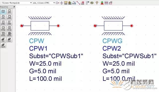
The use of simulation software, such as Keysight Technologies ADS, can provide appropriate parameters for various CPW and CPWG circuit designs, such as trace width, dielectric thickness, and spacing between ground planes, all of which can have a significant impact on final performance.
Solar Pump Inverter,Solar Pump Control Inverter,Frequency Inverter For Solar Pump,Single Phase Solar Pump Inverter
Zhejiang Kaimin Electric Co., Ltd. , https://www.ckmineinverter.com