Embedded engineers often use MCUs, ARMs, DSPs, and FPGAs to handle them. Once the system is designed, power is supplied to the power system. Although it can also run its well-designed programs, for newcomers, sometimes It may be inefficient, and often there is a problem that the supply current is insufficient or too large, causing such problems. The ten golden laws of this paper can easily handle the DCDC power conversion circuit design.
The first one, how to understand DC / DC power supply
The DC/DC power supply circuit is also called a DC/DC conversion circuit, and its main function is to perform input and output voltage conversion. Generally, the voltage conversion process in which the input power supply voltage is within 72V is called DC/DC conversion. Common power sources are mainly divided into vehicle and communication series and general industrial and consumer series. The former uses voltages of 48V, 36V, 24V, etc., and the latter uses a power supply voltage of 24V or less. Different application fields have different laws, such as 12V, 5V, 3.3V commonly used in PC, 5V 15V for analog circuit power supply, 3.3V for digital circuit, etc. Now FPGA and DSP also use voltage below 2V, such as 1.8V, 1.5. V, 1.2V, etc. Also known in the communication system as a secondary power source, it is provided with a DC input voltage from a primary power supply or a DC battery pack, and one or several DC voltages are obtained at the output after DC/DC conversion.
Second, need to know the DC / DC conversion circuit classification
DC/DC conversion circuits are mainly divided into the following three categories:
1 voltage regulator voltage regulator circuit. 2 linear (analog) voltage regulator circuit. 3 switching regulator circuit
The third, the simplest regulator circuit design
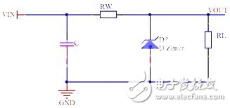
The voltage regulator tube voltage regulator circuit has a simple circuit structure, but has a poor load capacity and a small output power, and generally only provides a reference voltage for the chip, and does not use the power source. More commonly used is a shunt regulator circuit, the circuit diagram is shown in Figure (1),

When selecting a Zener tube, it can generally be estimated by the following formula: (1) Uz=Vout; (2) Izmax=(1.5-3)ILmax (3)Vin=(2-3)Vout This circuit is simple in structure and can be The input voltage is disturbed, but the output voltage cannot be adjusted arbitrarily because it is limited by the maximum operating current of the Zener tube. Therefore, the circuit is suitable for applications where the output voltage does not need to be adjusted, the load current is small, and the requirements are not high. The power supply voltage is not required to supply power to the chip.
Fourth, the reference voltage source chip regulator circuit
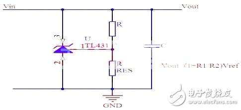
Another form of voltage regulator circuit, some chips have higher requirements on the supply voltage, such as the reference voltage of the AD DA chip. At this time, some commonly used voltage reference chips such as TL431, MC1403, REF02, etc. The TL431 is the most commonly used reference source chip with a good thermal stability of the three-terminal adjustable shunt reference. Its output voltage can be arbitrarily set to any value from Vref (2.5V) to 36V with two resistors. The most common circuit application is shown below, where Vo = (1 + R1/R2) Vref. Selecting different values ​​of R1 and R2 results in any voltage output from 2.5V to 36V, in particular, when R1 = R2, Vo = 5V.

Several other reference voltage chip circuits are similar.
Article 5: Circuit recognition of series-type regulated power supply
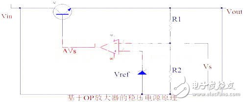
The series regulator circuit is one of the DC regulated power supplies. It is a commonly used DC power supply method before the appearance of the three-terminal regulator. Before the appearance of the three-terminal regulator, the series regulator usually has an OP amplifier and The Zener diode constitutes an error detection circuit, as shown in the following figure, in which the reverse input terminal of the OP amplifier is connected to the detection signal of the output voltage, and the forward input terminal is connected to the reference voltage Vref, Vs=Vout*R2/(R1+R2) ). Since the amplified signal ΔVs is a negative value, the voltage of the base of the control transistor is lowered, so the output voltage is reduced. Under normal conditions, Vref=Vs=Vout*R2/(R1+R2), and the ratio of R1 and R2 can be set. Determine the required output voltage value.
The figure shows that this is also the basic principle of the three-terminal regulator. In fact, the load size can be changed to a Darlington tube, etc. This series regulator circuit is composed of a DC power supply that is improperly processed. Easy to produce oscillations. Nowadays, engineers who do not have a certain analogy are generally not using this method. Instead, they use an integrated three-terminal regulator circuit for DC/DC conversion circuits.

Article 6. Common design schemes for linear (analog) integrated voltage regulator circuits
The linear regulator circuit design is mainly based on a three-terminal integrated voltage regulator. There are two main types of three-terminal regulators:
A fixed output voltage is called a fixed output three-terminal regulator. The general-purpose products of the three-terminal regulator are 78 series (positive power supply) and 79 series (negative power supply). The output voltage is the latter two of the specific models. The figures represent 5V, 6V, 8V, 9V, 12V, 15V, 18V, 24V and other grades. The output current is divided by 78 (or 79) followed by a letter. L represents 0.1A, M represents 0.5A, no letter indicates 1.5A, and 78L05 represents 5V 0.1A.
Another type of output voltage is an adjustable linear regulator circuit called an adjustable output three-terminal regulator. These chips represent the LM317 (positive output) and LM337 (negative output) series. The maximum input-output limit difference is 40V, the output voltage is 1.2V-35V (-1.2V--35V) continuously adjustable, the output current is 0.5-1.5A, and the voltage between the output terminal and the adjustment terminal is 1.25V. The terminal quiescent current is 50uA.
The basic principle is the same, and both use a series regulator circuit. In the linear integrated voltage regulator, since the three-terminal regulator has only three terminals, it has fewer external components, is convenient to use, stable in performance, and low in price, and thus is widely used.
Article VII, DCDC conversion switch type voltage regulator circuit design
The DCDC conversion circuits described above all belong to the series feedback regulator circuit. In this mode of operation, the regulator tube operates in a linear amplification state, so when the load current is large, the loss is relatively large, that is, the conversion low efficiency. Therefore, the power supply circuit using the integrated regulator is not very large, generally only 2-3W. This design is only suitable for low-power power circuits.
The DCDC conversion circuit designed by the switching power supply chip has high conversion efficiency and is suitable for a large power supply circuit. It has been widely used, and it is commonly divided into non-isolated switching power supply and isolated switching power supply circuit.
DCDC conversion switch type voltage regulator circuit design, DCDC conversion circuit designed by switching power supply chip has high conversion efficiency and is suitable for larger power supply circuits. It has been widely used, and it is commonly divided into non-isolated switching power supply and isolated switching power supply circuit. Of course, the basic topologies of switching power supplies include buck, boost, buck-boost and flyback, forward, bridge, and so on.
Non-isolated DCDC switching converter circuit design.
Isolated DCDC switch conversion circuit design.
Article VIII, non-isolated DCDC switch conversion integrated circuit chip circuit design
DCDC switch conversion integrated circuit chip, the use of this type of chip is very similar to the LM317 in Article 6. Here, L4960 is used as an example. Generally, the 50-Hz power transformer is used for AC-AC conversion, and the ~220V is reduced to the switching power supply. The input voltage range of the conversion chip is 1.2~34V, and the DC-DC conversion is performed by L4960. At this time, the output voltage can be adjusted to 5V, up to 40V, and the maximum output current can reach 2.5A (can also be connected to a high-power switch) Carry out the expansion), and built-in comprehensive protection functions, such as overcurrent protection, overheat protection, etc. Although the L4960 is similar to the LM317, the L4960 of the switching power supply is not as efficient as the LM317 of the linear power supply. The L4960 can output a maximum of 100W (Pmax=40V*2.5A=100W), but it is the most It only consumes 7W, so the heat sink is small and easy to make. Similar to the L4960, the L296 has the same basic parameters as the L4960, except that the maximum output current can be as high as 4A, and it has more protection functions and different package types. There are many such chips, such as LM2576 series, TPS54350, LTC3770 and so on. Generally, when using these chips, the manufacturer will use detailed instructions and typical circuits for reference.
Article IX, Circuit Design of Isolated DCDC Switching Power Supply Module
Commonly used isolated DC/DC conversions fall into three main categories: 1. Flyback transformation. 2. Forward conversion. 3. Bridge transformation
Commonly used single-ended flyback DC/DC converter circuits, there are many models of such isolated control chips. The typical representative of the control chip is the commonly used UC3842 series. This is a high-performance fixed-frequency current controller that is primarily used to isolate AC/DC, DC/DC converter circuits. The main application principle is that the circuit consists of a main circuit, a control circuit, a start circuit and a feedback circuit. The main circuit adopts a single-ended flyback topology, which is formed by adding an isolation transformer after the evolution of the buck-boost chopper circuit. The circuit has the advantages of simple structure, high efficiency, wide input voltage range and the like. The control circuit is the core of the entire switching power supply, and the quality of the control directly determines the overall performance of the power supply. This circuit uses peak current type double loop control, which is to add peak current feedback control to the voltage closed loop control system. This kind of scheme can choose the right transformer and MOS tube to make the power very large. Compared with the previous design schemes, the circuit structure is complicated, the component parameters are difficult to determine, and the development cost is high. Therefore, it is preferred when this scheme is needed. Cheaper DC/DC isolation modules on the market.
Article 10, DCDC switch integrated power module solution
Many microprocessors and digital signal processors (DSPs) require a core supply and an input/output (I/O) supply that must be ordered at startup. Designers must consider the relative voltage and timing of the core and I/O voltage sources during power-up and power-down operations to meet manufacturer-specified performance specifications. If the correct power sequencing is not available, latchup or excessive current consumption may occur, which may result in microprocessor I/O ports or memory, programmable logic devices (PLDs), field programmable gate arrays (FPGAs), or data conversion. The I/O port of the support device such as the device is damaged. Kernel power and I/O power tracking are required to ensure that the I/O load is not driven before the core voltage is properly biased. Now there are special power supply module companies to tailor some special switching power supply modules, mainly those that are small in size, high in power density, high in conversion efficiency, low in heat generation, and long in average fault-free working time. , reliable, lower cost and higher performance DC / DC power modules. These modules combine most or all of the components required to implement a plug-and-play solution and can replace up to 40 different components. This simplifies integration and speeds up the design while reducing board space in the power management section.
The most traditional and common non-isolated DC/DC power modules are still in a single in-line (SiP) package. These open framework solutions do make progress in reducing design complexity. However, the simplest is to use standard packaged components on a printed circuit board.
Article 11: Considerations for the selection of DCDC power conversion scheme
This article is also a summary of this article, it is very important. This article mainly introduces several commonly used design methods for DCDC power conversion regulator voltage regulator, linear (analog) regulator, DCDC switching regulator.
1 It should be noted that the voltage regulator voltage regulator circuit can not be used as a power supply, and can only be used for power supply without a power requirement. 2 The linear voltage regulator circuit has a simple circuit structure, but because of low conversion efficiency, it can only be used for low power stability. In the voltage power supply; 3 switching type voltage regulator circuit has high conversion efficiency and can be applied in high power applications, but its limitation is relatively complicated in circuit structure (especially high power circuit), which is not conducive to miniaturization. Therefore, in the design process, the appropriate design can be selected according to actual needs.
Gravity Die Casting Parts,Aluminum Die Casting,Die Casting Auto Parts,Led Housing Aluminum Die-Casting
Yangzhou Huadong Can Illuminations Mould Manufactory Co., Ltd. , https://www.light-reflectors.com