As an NFC tag chip that conforms to the ISO14443A protocol and the NFC Forum Type 2 Tag standard, the Infineon SLE66R01PN has 128 Bytes of user storage capacity, 7 Bytes of UID, more than 10,000 data read and write times and 10 years of data. save time.
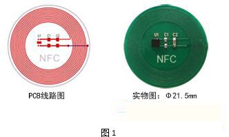
The Bluetooth pairing function is currently the mainstream application field of the NFC Forum Type 2 tag, and most of the applications adopt a design similar to the following FIG. 1 without trigger function. The premise of the work is that the Bluetooth module is turned on, the Bluetooth MAC address is stored on the NFC tag end, and the Bluetooth MAC is matched by NFC to achieve the purpose of Bluetooth pairing.

In other product applications, the Bluetooth module needs to be triggered by the NFC function to implement Bluetooth pairing. The SLE66R01PN chip itself does not have an FD trigger pin, so how to implement the trigger function, the following briefly introduces several comparison schemes (the chip uses 2.0x2.0x0.50mm, DFN4 pin package). Note: The J1 pin is connected to the GPIO port of the MCU of the Bluetooth module.
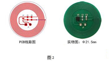
Solution 1: The peripheral circuit needs to be connected, as shown in Figure 2.

Pin J1 output voltage is output in AC mode. If you want to implement the trigger function, you need to add a rectifier circuit to the Bluetooth module circuit, and then connect to the GPIO of the Bluetooth module MCU.
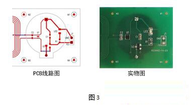
Option 2: Triode switch trigger, as shown in Figure 3.

An external power supply (Bluetooth module terminal power supply) is required as a trigger signal, and the electric field energy of the tag end is used as a switching signal for controlling the triode to realize triggering, and at this time, the output of the pin J1 is an external power supply voltage.
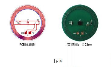
Solution 3: Diode voltage regulation trigger, as shown in Figure 4.

The principle is that the electric field energy is outputted by a diode chopping wave and a capacitor filter to achieve a stable trigger function. The diode regulator trigger module is the most cost-effective one of the current trigger schemes. It does not require an external power supply, simplifying the circuit design of the Bluetooth module.
In the actual circuit, the working voltage of the Bluetooth module MCU is generally 1.8V-3.6V, and the voltage output of the J1 pin of the scheme 3 can be stabilized at 1.8V-3.3V by adjusting, thereby realizing the function of stable triggering. Figure 5 (with the trigger function NFC module and Bluetooth module connection diagram)

Figure 5 Connection diagram of the NFC module and the Bluetooth module with trigger function
Compared with the current NFC chip with FD output pin on the market, SLE66R01PN has no disadvantages in Bom and circuit design. Because the NFC chip with FD output function uses the trigger function, it also needs to add a pull-up resistor to the tag or Bluetooth module circuit to implement the trigger function. Because the FD output of such chip is open-drain output, the Bluetooth module is required. The power supply acts as a trigger signal, and if the pull-up resistor is not applied, the trigger function cannot be implemented.
As the market demand for low-power design requirements such as wearables, headsets, and interactive game tags continues to increase, the market for NFC tag products with triggering capabilities will continue to expand.
For more intelligent Bluetooth information and technical articles, please refer to the electronic enthusiasts Designs of week column - " Let your smart Bluetooth product design no longer be resigned "

Electronic motors specilized for zebra blinds.
Zebra Blinds Motor,Multiple Limits Zebra Blind Motor,Radio Receiver Zebra Blind Motor,Zigbee Tubular Zebra Blind Motor
GUANGDONG A-OK TECHNOLOGY GRAND DEVELOPMENT CO.,LTD. , https://www.a-okmotor.com