In three minutes you know how to protect the input of the RF sampling ADC?
The design of any high performance ADC, especially the RF sampling ADC, input or front end, is critical to achieve the required system level performance. In many cases, RF sampling ADCs can digitally quantize signal bandwidths of hundreds of MHz. The front end can be active (using amplifiers) or passive (using transformers or baluns), depending on the system requirements. In either case, components must be carefully selected to achieve optimal ADC performance at the target frequency band.
IntroductionRF sampling ADCs are fabricated using deep sub-micron CMOS process technology, and the physical characteristics of semiconductor devices indicate that smaller transistor sizes support lower maximum voltages. Therefore, in the data book specifies the absolute maximum voltage that should not be exceeded for reasons of reliability, compared with the current mainstream RF sampling ADC, it can be found that this voltage value is smaller.
In receiver applications where the ADC is used to digitally quantize the input signal, system designers must pay close attention to the absolute maximum input voltage. This parameter directly affects the lifetime and reliability of the ADC. Unreliable ADCs may render the entire radio system unusable and the replacement cost may be very large.
To counteract the risk of overvoltage, the RF sampling ADC integrates a circuit that can detect high-level thresholds, allowing the receiver to compensate for gain adjustment through an automatic gain control (AGC) loop. However, if a pipelined ADC is used, the inherent architecture-related delays may cause the input to be exposed to high levels, potentially damaging the ADC input. This article discusses a simple way to enhance the AGC loop and protect the ADC.
Input schemaRF sampling ADCs can use a variety of different designs. The most common one is a pipeline architecture that uses multiple cascades to convert analog signals to digital signals. The first level is the most important and can be buffered or unbuffered. Which design to choose depends on design requirements and performance goals. For example, a buffered ADC typically has better SFDR performance in the frequency range but consumes more power than an unbuffered ADC.
The front-end design will also change depending on whether the ADC has a buffer stage. ADCs without buffers require additional series resistors to handle the input charge kickback, which also improves SFDR performance. Figure 1 and Figure 2 show a simplified diagram of the equivalent input circuit for the AD9625 unbuffered and AD9680 buffered RF sampling ADC. For simplicity, only single-ended inputs are shown.
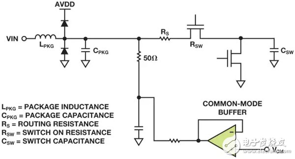
Figure 1. Equivalent circuit of unbuffered RF sampling ADC input
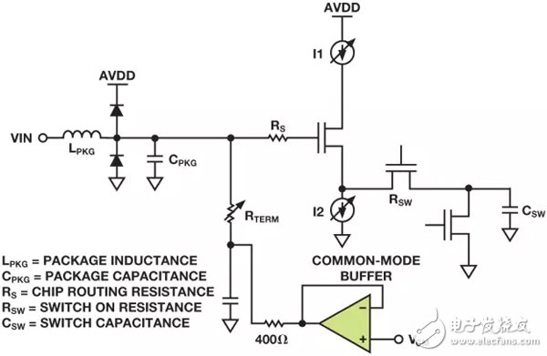
Figure 2. Equivalent circuit for buffering RF sampling ADC input
Regardless of the architecture, the absolute maximum absolute voltage at the ADC input is determined by the voltage that the MOSFET can handle. Buffered inputs are more complex and consume more power than unbuffered inputs. ADCs have many different types of buffers, the most common being source followers.
Failure mechanismThe fault mechanisms for buffered and unbuffered ADCs are different, but typically fail when the maximum allowable gate-source voltage ((VGS)) or drain-source voltage (VDS) is exceeded. These voltages are shown in Figure 3.
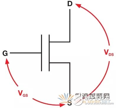
Figure 3. Key voltages of MOS transistors
For example, assuming that the VDS exceeds the maximum voltage allowed, a VDS breakdown fault occurs, which typically occurs when the MOSFET is in an off state and an excessive voltage with respect to the source is applied to the drain. If VGS exceeds the maximum voltage allowed, it can cause VGS breakdown (also called oxide breakdown). This usually occurs when the MOSFET is in a conducting state and an excessive voltage with respect to the source is applied to the gate.
Unbuffered ADC failure mechanismFigure 4 shows an unbuffered ADC input. The sampling process is controlled by the inverted clock signals Φ and Φ, which are the sample/hold signal of the MOSFET M1 and the reset signal of the MOSFET M2. When M1 turns on, M2 turns off and capacitor CSW tracks the signal (sampling or tracking mode). When M1 turns off, the comparator in MDAC makes a decision and M2 turns on, and capacitor CSW resets. This prepares the sampling capacitor for the next sample in the sampling phase. This circuit is usually in good working condition.
However, the high voltage input exposes M2 to a stress that exceeds its drain-source voltage. When the input high voltage is sampled (M1 on, M2 off), M2 is exposed to a large VDS, which is off for less than half of the sample clock, but even if it is only transient exposure. This will degrade the reliability of the circuit and cause the ADC to fail over time. In reset mode (M1 is off, M2 is on), there is an input signal on the drain of M1, which is exposed to a large VDS voltage.
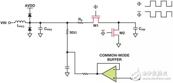
Figure 4. Failure Mode of Unbuffered ADC Input
Buffered ADC failure mechanismFigure 5 shows a buffered ADC input. The same clocking scheme applies to the sample and reset signals. Regardless of the phase, currents I1 and I2 are generated when the gate of buffer M3 is exposed to a high voltage input. The current source I1 is implemented using PMOS transistors, and I2 is implemented using NMOS transistors. The high voltage on the M3 gate causes excessive VDS in the I1 and I2 MOSFETs. In addition, the high voltage on the M3 gate can also cause breakdown of the oxide layer.
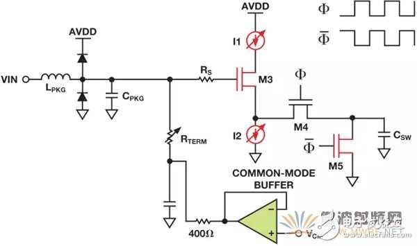
Figure 5. Buffering ADC Input Fault Mode
The breakdown mechanism of buffered and unbuffered ADCs is different, so the absolute maximum input voltage is also different, as shown in Table 1.
Table 1. Absolute Maximum Specifications for Buffered and Unbuffered ADCs
ADC process
(nm) input structure absolute maximum
Input voltage (V) differential swing
(V pp)
14-bit 105 MSPS350 buffer 79.2
14 bit 125 MSPS180 unbuffered 2.04.5
16-bit 250 MSPS180 buffer 3.66.0
12-bit 2.5 GSPS65 unbuffered 1.524
14 bit 1.0 GSPS65 buffer 3.24.6
TVS diode protection ADC input
There are several ways to protect the ADC input from high voltage. Some ADCs (especially RF sampling ADCs) have built-in circuitry that can detect the input voltage and report when the set threshold is exceeded. As described in the data sheet, there is some delay in the fast detection output, so it will still cause the ADC input to leak under high voltage in a short time.
Transient Voltage Stabilizer (TVS) diodes can limit excessive voltage but can affect ADC performance during normal operation. Figure 6 shows an overvoltage protection circuit using a TVS diode.
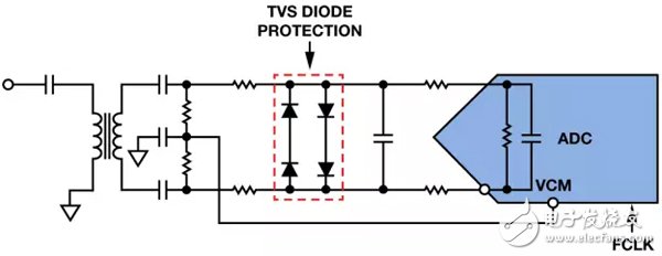
Figure 6. ADC front-end circuit with TVS diode protection
Although TVS diodes protect the ADC input by clamping excess voltage, they can greatly degrade the harmonic performance. Figure 7 shows a FFT comparison of a front-end band with and without a TVS diode for a 14-bit, 250-MSPS unbuffered ADC with a 30 MHz, –1 dBFS input.
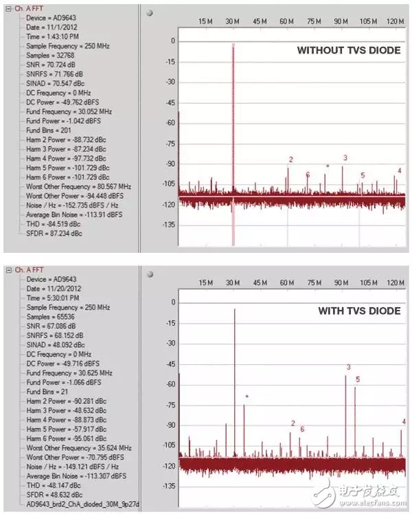
Figure 7. FFT comparison of ADC front-end circuit with and without TVS diode protection
TVS diodes can greatly degrade odd harmonic performance because they act as a reverse biased diode when they do not act as a clamp. The PN diode has a junction capacitance CJ0 that interacts with the nonlinear recoil current generated by the internal switching action of the ADC to produce a voltage signal that is mixed with the analog input signal. This mixed signal is sampled inside the ADC, generating a very large third harmonic. The time domain curve under overvoltage conditions (Figure 8) shows the clamp-cut function of TVS diodes. This does not mean that TVS diodes are not suitable for protecting the ADC input, but the diode specifications must be carefully considered in order to achieve the performance requirements. A more complete consideration must be given when selecting the diode type and its parameters.
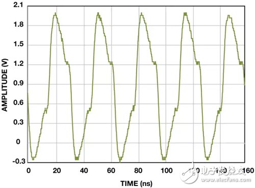
Figure 8. TVS diode protection in the front-end circuit causes clipping
Schottky diode protection RF sampling ADC inputWhen the bandwidth and sampling rate reach GHz and GSPS levels, RF sampling ADCs can simplify radio receiver designs because they do not require many mixer stages before the ADC, but this can make the ADC input susceptible to over-stress. Figure 9 shows a typical front-end design for an RF sampling ADC, driven by an amplifier. The next-generation amplifiers are specifically designed to interface with these ADCs, with fast attack response input discipline, and can be configured to attenuate the output to a predetermined gain through a Serial Peripheral Interface (SPI) configuration. The fast attack response pin can be configured to respond to the fast detection output of the RF sampling ADC. The ADA4961 is an example of a next-generation amplifier with fast attack response. The AD9680 and AD9625 are examples of RF sampling ADCs with fast detection capabilities.
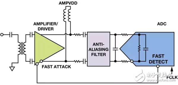
Figure 9. Amplifier-driven fast-response RF sampling ADC with fast detection
The topology in Figure 9 works well as long as the input voltage is within a reasonable range. For example, if the receiver's input receives a burst of high-voltage signals, the output of the amplifier will rise to the amplifier's supply rail voltage level (5 V in this example). This will generate a large voltage swing that exceeds the absolute maximum rated voltage at the ADC input. The fast detection function has a certain delay (28 cycles or 28 ns for the AD9680-1000), so waiting until the fast sense logic output tells the amplifier to set a fast attack response, the ADC is already exposed to high voltage for a few clock cycles. This may reduce the reliability of the ADC, so system designs that cannot withstand this risk must use the second protection mode. A fast-response Schottky diode with very low device and parasitic capacitance works well in this situation. The specific parameters of a particular diode can be found in the data sheet.
Reverse Breakdown Voltage (VBR)—The maximum input voltage at the input pin of the AD9680—about 3.2 V relative to AGND, so a reverse breakdown voltage of 3 V is selected for this diode.
Junction Capacitor (CJ0) - The diode capacitance should be as low as possible to ensure that the diode does not affect the ADC's ac performance (SNR/SFDR) during normal operation.
Figure 10 shows the passive front end with the Schottky diode before the ADC. The passive front end makes it easy to demonstrate that the Schottky diode protects the ADC input without affecting the ac performance.
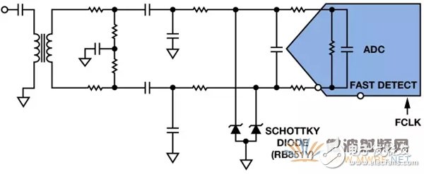
Figure 10. Passive front-end circuit showing RF sampling ADC and Schottky diode
This RF sampling ADC has been tested to input signals up to 2 GHz, so an RF Schottky diode (RB851Y) was chosen. Table 2 shows the key parameters of the RB851Y; it shows that the device is suitable for this application. The test results show that the diode prevents the ADC input voltage from exceeding its absolute maximum voltage of 3.2 V (vs. AGND). Figure 11 shows a single-ended input (the VIN+ pin of the ADC) exposed to high voltage (185 MHz). The Schottky diode clamps the voltage to about 3.0 V (with respect to AGND) to prevent the ADC input from reaching the 3.2 V limit. Figure 12 shows the differential signal at the input of the AD9680 with a Schottky diode clamp.
Table 2. Key Parameters of Schottky Diodes Used to Protect RF Sampling ADC Inputs
Parameter Value Unit Notes
Reverse voltage (VR) 3VAD9680 data sheet, absolute maximum rated voltage is VIN± = 3.2 V
Capacitance between endpoints
(CJ0, or Ct) 0.8pF Less Impact on ADC Performance Under Normal Conditions
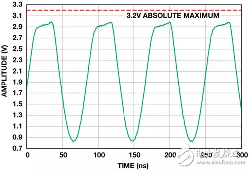
Figure 11. Schottky Diode Clamped Single-Ended ADC Input
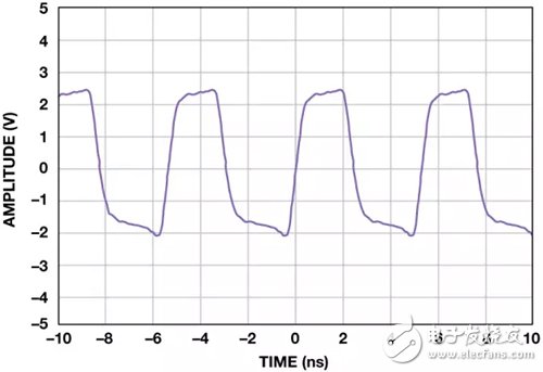
Figure 12. Schottky Diode Clamp AD9680 Differential Input Signal
Next, we measure normal operating performance. The AD9680 is controlled as suggested in the data sheet, but the input is modified as shown in Figure 10. The analog input frequency varies from 10 MHz to 2 GHz. The ultra low value of CJ0 should not affect the SNR and SFDR performance of the ADC.
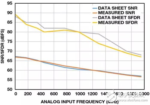
Figure 13. Relationship between SNR/SFDR and Analog Input Frequency with Schottky Diode Protection for the AD9680
The Schottky diode does not affect the SNR performance at all, but the SFDR deviates from the expected value at some frequencies, as shown in Figure 13. This may be due to differential signal mismatch or ADC kickback. The evaluation board is designed from a wide frequency range from dc to 2 GHz, so when it works well in the whole frequency band, some components may interact with Schottky diodes at specific frequencies.
Most applications will not use the entire 2 GHz band, so you can tune the front end to the desired target signal bandwidth by modifying the overvoltage protection input circuit. Careful selection of the Schottky diode protects the ADC input, allowing the system designer to use an amplifier with the latest fast attack response and fast detection to drive the front-end circuit, as shown in Figure 14.
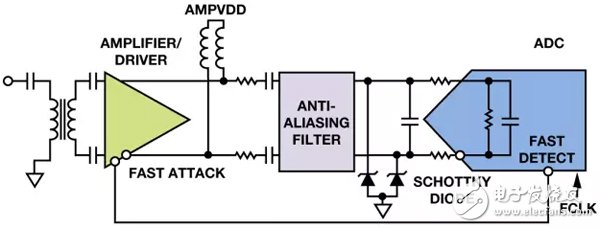
Figure 14. ADA4961 Driving the AD9680 (Display RF Sampling ADC and Schottky Diode)
in conclusionThis article discusses how to use a Schottky diode to protect the RF sampling ADC input from overvoltage stress. Careful review of the diode data sheet parameters is critical. In order to achieve the best target frequency band performance, the implementation of this circuit needs to be planned. The fast detection output of the RF sampling ADC can be combined with the fast attack response function of the latest amplifiers to set the automatic gain control loop.
Bacteria are everywhere in our daily lives. Mobile phones have become an indispensable item for us. Of course, bacteria will inevitably grow on the phone screen. The antimicrobial coating used in our Anti Microbial Screen Protector can reduce 99% of the bacterial growth on the screen, giving you more peace of mind.
Self-healing function
The Screen Protector can automatically repair tiny scratches and bubbles within 24 hours.
Clear and vivid
A transparent protective layer that provides the same visual experience as the device itself.
Sensitive touch
The 0.14mm Ultra-Thin Protective Film can maintain the sensitivity of the touch screen to accurately respond to your touch. Like swiping on the device screen.
Oleophobic and waterproof
Anti-fingerprint and oil-proof design can help keep the screen clean and clear.
If you want to know more about Anti Microbial Screen Protector products, please click Product Details to view the parameters, models, pictures, prices and other information about Anti Microbial Screen Protector products.
Whether you are a group or an individual, we will try our best to provide you with accurate and comprehensive information about Anti Microbial Screen Protector!
Antimicrobial Screen Protector, Anti-microbial Screen Protector, Anti-bacterial Screen Protector, Antibacterial Screen Protector,Anti-microbial Hydrogel Screen Protector
Shenzhen Jianjiantong Technology Co., Ltd. , https://www.tpuprotector.com