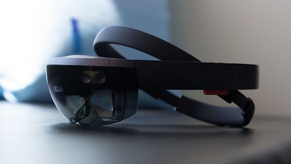
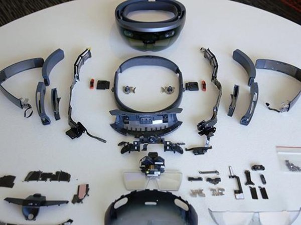
Microsoft finally revealed the internal structure of its augmented reality head-up HoloLens. Although as early as April someone had dissected the HoloLens development version, Microsoft has kept HoloLens's dedicated holographic processing unit (HPU) secret. Earlier this year, Microsoft disclosed most of HoloLens' specifications. The dedicated HPU's design is mainly used for most data processing, thus greatly reducing the burden on the CPU and GPU. Microsoft's custom-designed HPU can process all the data from cameras and sensors in real time, and the ability to use gestures precisely also depends on its power.

HoloLens dismantling diagram
This week at the HOTCHIPS conference in California, Microsoft's equipment engineer Nick Baker introduced what exactly the HPU is and how powerful it is. The Microsoft-customized HPU is a 28-nanometer coprocessor built by TSMC and consists of 24 cores of Tensilica DSP (Digital Signal Processing). It has about 65 million logic gates, 8MB of SRAM and an additional 1GB of low-power DDR3 memory. The device also has a separate 1GB of memory that can be used with the Intel Atom Cherry Trail processor. The HPU itself can handle approximately one trillion calculations per second.

Microsoft's HPU power consumption is very low, it uses less than 10W of energy. The purpose of this is also to handle very power-hungry gesture tracking and contextual awareness. It also includes PCIe and standard serial interfaces, and Microsoft has added 10 custom instructions to accelerate the special instructions of the HoloLens augmented reality algorithm.
Microsoft has now publicly launched HoloLens, which has two sales plans for developers and commercial customers. The device costs $3,000.