What are the features of the 8251a? How does the _8251a work in serial communication?

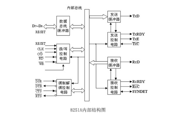
The receiver includes a receiver buffer and receive control logic. The function of the receiver is to receive the serial data on the RXD pin and convert it into parallel data in a prescribed format, which is stored in the data bus buffer.
1 receive buffer
The receive buffer consists mainly of shift registers and digital registers. The receiver receives the serial data transmitted to the RXD (receive data input) pin, and checks and processes special bits (parity bit, stop bit, etc.) and characters (synchronization character) of the serial data stream. The format converts serial data into parallel data in a buffer.
The receive shift register and the receive data buffer form a double buffer structure.
2 Receive control logic
This section controls the reception of serial data, including three control lines:
RXRDY (Receiver Ready) Receiver ready, output, active high.
RXC (Receiver Clock) receiving clock, input.
SYNDET/BRKDET (SYNchronous DETect/BreaK DETect) Synchronous detection/breakpoint detection, output/input, active high.
(2) TransmitterThe transmitter includes two parts: a transmit buffer and a transmit control logic.
1 send buffer and send process
The transmit data buffer receives the parallel data sent by the CPU, converts it into a serial data stream according to the data format specified by the initialization program, and sends it to the transmit shift register, which is transmitted from the TXD pin on the falling edge of TXC.
The transmit data buffer and the transmit shift register compose the transmitted double buffer structure.
2 send control logic
This section controls the serial data transmission operation, including 3 control lines:
TXRDY (Transmitter ReaDy) Transmitter ready, output, active high.
TXE (Transmitter Empty) Transmitter Empty, Output, Active High.
TXC (Transmitter Clock) send clock, input.
(3) Read/write control logicThe read/write control logic receives the relevant control signal from the CPU and determines the operation of the 8251A accordingly. There are 6 external leads in this section.
CLK clock, input.
RESET reset, input, active high. RESET is active, 8251A is forced to reset to idle state. Only after re-initialization can you get out of idle.
 (Chip Select) chip select, input, active low.
 (Control/Data) Control/Data signal, input.
 (Read) Read, input, active low.
 (Write) Write, Input, Active Low.
The data bus buffer is a tri-state, bidirectional, 8-bit buffer that is connected to the system's data bus via pins D7D7 to D0D0 and is the interface between the 8251A and the system data bus. The data bus buffer includes:
1 Status word buffer register, registering various working states of the 8251A receive/send operation.
2 Send a data buffer register to temporarily store data or control words sent by the CPU. The 8251A does not have an independent control register. The write control command and the transmitted data share one register.
3 Receive data buffer register, temporary storage received to the CPU data.
(5) Modem control logicIn the long-distance communication, TXD end data of 8251A is modulated by the modulator and then sent to the transmission line. After being demodulated, the signal sent from the transmission line is sent to the RXD end of the 8251A. In order to transmit data correctly between the 8251A and the modem, the 8251A modem control logic generates four corresponding contact signals as follows:
 (Data Terminal Ready) Data Terminal Ready, Output, Active Low.
 (Data Set Ready) Modem Ready, Input, Active Low.
 (Request To Send) request to send, input, active low.
 (Clear To Send) Allows send, input, active low.
When the 8251A is not connected to the modem but other peripherals, these four lines can be used as control lines for data transmission.
What role and characteristics does it play in 8251a serial communicationThe 8251A is a programmable universal synchronous/asynchronous receiver/transmitter. It is usually used as a serial communication interface and is widely used in microcomputers with the Intel80X86 CPU. Its basic function is:
(1) It is a full duplex, double buffered receiver/transmitter.
(2) There are two ways to work, can work in synchronous or asynchronous work. In the synchronous mode, the baud rate is in the range of 0 to 64K. In the asynchronous mode, the baud rate is in the range of 0 to 9.2K.
(3) In synchronous mode, the character can be selected as 5-8 bits, parity bit can be added, and the synchronization character can be automatically detected.
(4) In asynchronous mode, characters can be selected as 5-8 bits, parity bits can be added, a start bit is automatically added for each character, and 11, 1.51.5, or 22 stop bits can be selected by programming.

1, asynchronous work methods:
The CPU issues a receive command, and the receiving circuit monitors the RxD side, finds a start bit, and begins a character reception process. Under the action of the receiving hour hand, the received data enters the receiving shift register serially, is shifted and carries on the parity check, then deletes the stop bit, obtains the parallel data, receives the data buffer through the on-chip bus, waits for the CPU to read Taken while the RxRDY pin is set high and the RxRDY bit of the status register is 1
2, synchronous work methods:
The same way of working is divided into internal synchronization and external synchronization:
3, work in the internal synchronization:
The CPU issues an enable and receive search command, detects the RxD pin, and sends the received data bit to the shift register and compares it with the content of the synchronous character register. If they are different, they continuously receive and perform a shift comparison operation, knowing that the same occurs. Then the SYNDET set high, indicating that synchronization occurs. If it is double synchronization, two characters are required.
4, work outside synchronization:
The synchronous character is monitored by an external circuit. When a synchronization character is found, a high level is input from the synchronous input SYNDET to inform that the 8251A and 8251A are out of the search process for the synchronous character, and the high level needs to maintain a receiving clock period.
After synchronization is reached, the 8251A uses the receive clock to sample RxD and receive synchronous frame format data. The acquired data is sent to the shift register. When the number of bits reaches a bit defined by one character, the contents of the shift register are sent to the receive data buffer through the on-chip bus. At the same time, the RxRDY pin is set high and the status register The RxRDY bit is 1, indicating that an available character has been received.
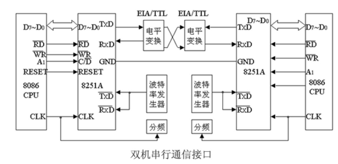
Application Example 8251AExample: Hardware connection and software programming for two-machine serial communication between two microcomputers in a microcomputer system.
(1) Requirements
Serial communication between the two A and B computers, A machine to send, B machine to receive. It is required that the application developed on the A-machine (whose length is 2DH) be sent to B. The two parties use start-stop asynchronous mode. The data format of the communication is 8 characters, 2 stop bits, a baud rate factor of 64, no parity, and a baud rate of 4800. The CPU and the 8251A exchange data by query. The port address assignment of the 8251A is: 309H is the command/status port, and 308H is the data port.
(2) Analysis
Because it is a short-distance transmission, it is not necessary to set a MODEM. The two microcomputers can directly connect through the RS-232 standard interface. At the same time, the query I/O method is adopted. Therefore, in the receiving/sending program, it is only necessary to check whether the status of the send/receive ready status is set or not, and l bytes can be transmitted and received.
(3) Design
1 hardware connection
Based on the above analysis, both microcomputers are treated as DTEs (Data Terminal Equipment), and communications can be performed using the simplest transmission lines TxD, RxD, and GND. Using 8251A as the main chip of the interface and then configure a small number of additional circuits, such as the baud rate generator, RS-232C and TTL level conversion circuit, address decoding circuit, etc. can constitute a serial communication interface.
![]()

2 software programming
It can be seen from the question that the receiving and sending programs should be written separately. Each program section includes the 8251A initialization, status query, and input/output sections. When the receiver/sender's 8251A is initialized, it is first necessary to determine the mode for selecting the control word and the work command control word. According to the requirements in the question, there are:
The sender's mode selection control word is 11001111B=CFH, and the work command control word is 00111110B=37H.
The receiver's mode selection control word is 11001111B=CFH, and the work command control word is 00010100B=14H.
Sender's sender (omit STACK and DATA segments)
CSEG SEGMENT
ASSUME CS: CSEG
TRA PROC FAR
START: MOV DX,309H ; Control port
MOV AL. 00H ; Empty operation
OUT DX,AL
MOV AL,40H ; Internal Reset
OUT DX,AL
NOP
MOV AL,0CFH ;Mode word (asynchronous, 2 stop bits, 8 characters, no parity, baud rate factor 64)
OUT DX, AL
MOV AL, 37H ; Command word (RTS, ER, RxE, DTR, and TxEN are all set to 1)
OUT DX, AL
MOV CX,2DH ; Bytes transmitted
MOV SI, 300H; Send Area First Address
L1: MOV DX,309H ; Status port
IN AL, DX; Check status bit D. (TxRDY)=1?
TEST AL, 38H; Check Error
JNZ ERR ;Error handling
AND AL,01H
JZ L1 ; Waiting to send if not ready
MOV DX,308H ;Data port
MOV AL,[SI] ;Send ready for sending, send 1 byte from send area
OUT DX, AL
INC SI ; Modify memory address
DEC CX ; number of bytes minus 1
JNZ L1 ; Not sent out, continue
ERR: (slightly)
MOV AX, 4C00H ; Sent out, back to DOS
INT 21H
TRA ENDP
CSEG ENDS
END START
Receiver receiving program (omit STACK and DATA segments)
SCEG SEGMENT
ASSUME CS:REC
REC PROC FAR
BEGIN: MOV DX,309H ; Control port
MOV AL, 0AAH ; Empty operation
OUT DX, AL
MOV AL,50H ; Internal Reset
OUT DX, AL
NOP MOV AL,0CFH ;mode word
OUT DX, AL
MOV AL, 14H ; Command word (ER, RxE set to 1)
OUT DX, AL
MOV CX,2DH ; Bytes transmitted
MOV DI, 400H; receiving area first address
L2: MOV DX,309H ; Status port
IN AL, DX; Status Bit D2 (RxRDY) = 17
TEST AL, 38H; Check Error
JNZ ERR ; Turn error handling.
AND AL, 02H
JZ L2 ; Receive not ready, wait
MOV DX,308H ;Data port
IN AL, DX ; Receive ready, receive 1 byte
MOV [DI], AL ; Save to receive area
INC DI ; modify memory
LOOP L2 ; Not completed, continue
ERR: (slightly)
MOV AX,4C00H ;Has been received, the program ends, exit
INT 21H ; Return to DOS
REC ENDP
CSEG ENDS
END BEGIN
With 15+ years manufacturing experience for Portable Power.
Supply various portable charger for iPhone, Airpods, laptop, radio-controlled aircraft ,laptop, car and medical device mobile device, ect.
From the original ordinary portable power source to Wireless Power Bank, Green Energy Solar Power Bank, Magnetic Mobile Power, Portable Power Stations and other products continue to innovate.
Avoiding your devices run out of charge, Portable Chargers to keep your mobile device going.
We help 200+ customers create a custom mobile power bank design for various industries.
Wireless Earphones,Wireless Headphones,Best Wireless Headphones,Best Bluetooth Earphones
TOPNOTCH INTERNATIONAL GROUP LIMITED , https://www.itopnoobluetoothes.com