Ultraviolet detection technology is another dual-use photoelectric detection technology developed after infrared and laser detection technology. As early as the 1950s, people began research on UV detection technology. The EUV detector uses the 30.4 nm wavelength extreme ultraviolet imaging technology to image the Earth's plasma layer, which can be used to obtain the distribution of the entire magnetic layer around the Earth for space environment detection and study of changes during solar disturbance.
On October 24, 2007, China’s “嫦娥†No. 1 satellite was successfully launched, marking China’s entry into the ranks of countries with deep space exploration capabilities. At present, the EUV imaging experiment of the moon-based Earth plasma layer is carried out in the second phase of the “Exploration of the Moon†project to study the changes in the Earth's space environment and provide observational data for the catastrophic environmental changes.
Our research group has carried out technical research on the extreme ultraviolet imaging detection system, and has achieved good results in anode design and circuit signal processing.
1 Structure of Vernier anode detectorAnode detectors can be divided into two types according to position sensitivity: one is a unit type, such as MAMA type; the other is continuity, such as resistance anode, WSA, Delay-line, Vernier, and the like. Among them, Vernier anode has higher photon counting rate and position resolution than other anodes. Therefore, this paper mainly introduces Vernier anode.
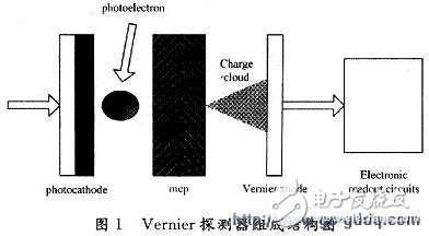
The anode detector is mainly composed of a photocathode, an MCP, a position sensitive anode and an electronic readout circuit. The basic structure of the anode detector is shown in Figure 1. The single-photon light source reaches the photocathode through the input window to generate electrons, and then the electron cloud is multiplied by the V-type cascade MCP, and reaches the Vernier anode under the action of the acceleration electric field to form a plurality of electronic pulses. The multiplexed signal is processed by the electronic readout circuit and decoded by software to form a grayscale image.
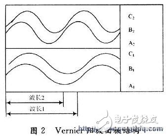
The anode panel structure used to collect the electron cloud is shown in Fig. 2. A total of six electrodes collect charges, which are insulated from each other. In the lateral direction, the area of ​​each electrode changes sinusoidally, and they differ by 120°, and the phase of the sinusoid changes linearly with the lateral direction. The amount of charge Q collected on each electrode also varies sinusoidally with position, and the amount of charge Q is proportional to the electrode area SQ of the collected charge, since the sinusoidal wavelength is much larger than the electrode width, within each electrode area covered by the electron cloud The position of the electron cloud centroid is proportional to the electrode width, so the phase value θ of the centroid position on the electrode can be obtained, and the abscissa x value can be obtained by the θ value. When the x values ​​of the two sets of electrodes are the same, the photon can be obtained in the anode panel. The coordinate position on the top.
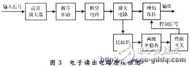
The electronic readout circuit is mainly composed of a charge sensitive preamplifier, a filter shaping amplifier circuit and a peak hold circuit. The charge sensitive preamplifier is mainly used to convert the signal output from the anode into a voltage signal; the filter shaping circuit is to make the shape of the signal satisfy the quasi-Gaussian waveform to meet the needs of subsequent processing and improve the signal to noise ratio of the signal; the peak hold circuit is The peak of the signal is broadened to improve the peak accuracy obtained. The block diagram is shown in Figure 3.
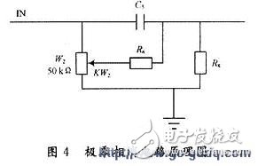
In the preamplifier circuit, in order to improve the input impedance and reduce noise, a low noise junction field effect transistor is used as an input stage of the charge sensitive preamplifier, such as 2SKl52, 2N4416. The feedback resistance and capacitance are set to RF=500 MΩ, Cf=1 pF, so τ=500&TImes;106&TImes;10-12=500μs, the tail of the output waveform is long, and pulse accumulation is easy to occur. In order to increase the count rate, CR differential processing is required, as shown in FIG. Its transfer function is  In the formula
  In the design, when τ1=τ, the goal of zero-zero cancellation is achieved. In Figure 4, C5 = 1 000 pF, R6 = 1 MΩ, and W2 = 50 kΩ. Different photon rates incident on the system have different requirements for integration time. Different integration times can be obtained by selecting different R8 values. At C = 1 000 pF, when τ2 = 1 μs, R8 = 1 kΩ; when τ2 = 2 μs, R8 = 2 kΩ; when r2 = 10 μs, R8 = 10 kΩ. Jumpers are used in the actual circuit to achieve the choice of R8.
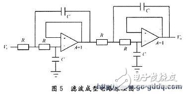
The waveform output by the pole zero cancellation circuit cannot directly sample the circuit, and its waveform must be improved. In order to meet the needs of the acquisition card for the signal waveform, improve the signal-to-noise ratio, and accurately obtain the pulse peak data, it is necessary to further filter and shape the signal. According to the discussion of the optimal filter, the symmetric infinite wide apex pulse has the best signal-to-noise ratio, and the Gaussian waveform has the above characteristics. The top of the pulse is relatively flat, so the pulse is generally shaped by a Gaussian or quasi-Gaussian waveform. Using the circuit structure shown in Figure 5, a two-stage active low-pass filter is used. At C = 1 000 pF, values ​​are taken for different integration times, when τ2 = 1 μs; when R = 1 kΩ, when τ2 = 2 μs, R = 2 kΩ; when τ2 = 10 μs, R = 10 kΩ. Similarly, R uses jumpers to achieve values.
The basic principle of the peak hold circuit is shown in Figure 6. When the input signal is larger than the threshold, the comparator 1 outputs a high level trigger flip-flop 1 output Q is high level, the flip-flop 2 output Q is high level, to control the logic level of the LF398, so that the LF398 is in the adopted state.
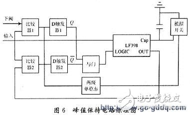
When the signal reaches the peak value, Comparator 2 outputs a high level, causing the AND circuit to output a low level, at which time LF398 is in a hold state, thereby maintaining the peak value of the signal. The control circuit is mainly completed by two-stage monostable. When the comparator 1 outputs a high level, the rising edge triggers the 1-level monostable state, and the temporary stabilization time of the output can be adjusted by the external resistor for the length of time. The transient falling edge triggers the 2-level monostable, and the high level of the output triggers the analog switch, causing the LF398's holding voltage capacitor to discharge quickly.
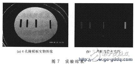
3 ConclusionWhen testing the circuit, the circuit is connected to the UV single photon counting imaging system built by the research team. The output waveform of each circuit is observed by the Tek DPO 4104 oscilloscope to meet the quasi-Gaussian distribution, and the system is used to image the 4-hole mask. Fig. 7(a) is a physical view of a 4-hole mask, with the distance between the holes being 7 mm, 9 mm, 15 mm and a hole diameter of about 2 mm. Experimental conditions: The light source is a low-pressure mercury lamp, two MCPs are applied with a voltage of 2 280 V, a voltage between the MCP and the anode is 300 V, the distance between the two MCPs is 50 μm, and the distance between the MCP and the anode is 15 mm. When the degree of vacuum reaches 1.0 & TImes; 10-4 Pa, the pulse signal output from the anode is connected to the electronic readout circuit. The circuit parameters used in this experiment are: the sensitivity of the preamplifier A=1 V/pc, the pulse shaping time is 2μs, the voltage amplification factor is 4 times, and the pulse half-width of the pulse output is measured by the oscilloscope to be 5μs, the voltage amplitude The range of the acquisition card is 0 to 10 V. After collecting the voltage peak from the acquisition card, the grayscale image obtained by software decoding is shown in Fig. 7(b), and it can be seen that the obtained image is consistent with the real object.
A signal processing circuit of Vernier anode detector is designed. The signal voltage amplitude and signal-to-noise ratio processed by this circuit meet the design requirements of the anode detector. Through the experimental test of the designed circuit, the requirements of the single photon detection imaging system can be met, and the feasibility of the electronic readout circuit is verified.
Inverters Converters,Inverter Ac Converters,Hybrid Inverter Converters,Frequency Inverters Converters
GuangZhou HanFong New Energy Technology Co. , Ltd. , https://www.gzinverter.com