PROTEUS is tool software from UK companies and is widely used around the world. Compared with other tools, the biggest feature of this software is that it can simulate the microcontroller. It can be programmed directly on the schematic-based virtual prototype EDA and enables real-time debugging of the software source code level. You can also see the effect of input and output after running. But now everyone has only noticed PROTEUS's simulation of the microcontroller and how to debug it with Keil. In fact, PROTEUS can also perform the circuit simulation of PLD.
PLD (Programmable Logic Device) is a semi-finished product of digital integrated circuits. It integrates a large number of basic logic elements such as gates and flip-flops in a certain arrangement on the chip. Users can use a certain development tool to process them. That is, according to the design requirements, these on-chip components are connected to complete a certain logic circuit or system function, and become an application-specific integrated circuit that can be used in practical electronic systems.
The general PLD design software can only perform the sequential logic simulation of the PLD chip, while the PROTEUS can perform the PLD circuit simulation and simulate the actual operation of the designed PLD chip in the circuit.
We use the GAL16V8 to design a three-eighth translator commonly used in the microcontroller system, and then in the PROTEUS by observing the GAL16V8 thirty eight decoder input and output corresponding relationship to complete the PLD circuit simulation.
2. Design of PLDFirst use the Protel 99SE to complete the PLD design.
The completed PLD schematic is as follows:
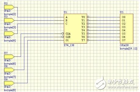
Figure 1 PLD diagram drawn
This is a 3-8 decoder PLD file. The input signal is the target 2, 3, 4 of the target, the output signal is the 12-19 pin of the target, and the 6-8 pin is the enable control.
Protel 99SE PLD schematic design is the same as the general schematic, but there are several points that need attention:
After the PLD physics diagram is generated, the two PLD component libraries (PLD_Devices.lib, PLD_Symbols.lib) are automatically added in the schematic diagram. The drawing of the PLD circuit diagram must use the components of these two libraries.
When plotting a PLD schematic, the input/output port (input: IPAD, output: OPAD, input/output: IOPAD) elements must be placed and the pins designated by these elements represent the pins of the target device.
After the input/output port components are placed, they must be numbered and the pin number of the target device to which the port component is connected.
After completing the PLD schematic, select [PLD]/[Compile] to compile and generate files in various formats:
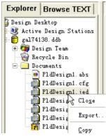
Figure 2 compiled and generated various files
Open the generated .jed file, right click, select [Export...] item in the popup window, and select the output destination of the .jed file.
This completes the design of the PLD file.
3 Proteus simulation of PLDStart Proteus and draw the circuit diagram.
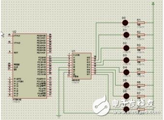
Figure 3 Proteus simulation circuit diagram
The LED display in the circuit shows the LED lighting when using a low level. In the circuit I1-I3 is the GAL16V8 input port. When the port is high level, it is 1; when it is low level, it is 0; IO0-IO7 is the output port; the output port is: when the LED light is on, the port output is low level 0; when it is off, it is high power. Flat 1.
To enable PLD components to be emulated, the compiled .jed file must also be added to the PLD component in the circuit: Move the mouse to U1 (16V8), right-click, select the component, and then left-click, bring up the "Element Properties" In the dialog box, in the Properties dialog box, add the .jed file in the "JEDEC Fuse Map File:" in the window:
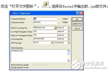
Figure 4 16V8 component properties
From the design of the previous PLD, the truth table of the 3-8 decoder is available:
Input signal output signal
I3 I2 I1 IO7 IO6 IO5 IO4 IO3 IO2 IO1 IO0
0 0 0 1 1 1 1 1 1 1 0
0 0 1 1 1 1 1 1 1 0 1
0 1 0 1 1 1 1 1 0 1 1
0 1 1 1 1 1 1 0 1 1 1
1 0 0 1 1 1 0 1 1 1
1 0 1 1 1 0 1 1 1 1 1
1 1 0 1 0 1 1 1 1 1 1
1 1 1 0 1 1 1 1 1 1 1
Table 1 3-8 Decoder Truth Table
In order to observe the correspondence between the input and output of 16V8, we will change the ports P2_2, P2_1, and P2_0 connected to I3, I2, and I1 according to the sequence in the truth table in the AT89C52 program (see appendix). Whether the LED lights are attached by IO0 to IO7.
After adding the SCM program to the AT89C52, click the Play button in the Proteus to view the circuit simulation result: When the input values ​​of I1, I2, and I3 are changed according to the program setting, 000-111 in the truth value table, the corresponding LED lights are output. According to the corresponding relationship in the truth table from IO0 to IO7 turn on, as shown below. Describe the correct decoding of the 38 decoder designed by the PLD device 16V8.
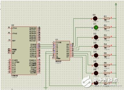
Figure 5 decoding circuit corresponding to the input / output screenshot
4. ConclusionThe combination of single-chip microcomputer and PLD is a kind of way that the current embedded design often adopts one. However, if you want to test the hardware circuit and system debugging is more troublesome, because to carry out these two processes must be completed after the completion of the circuit board, component welding is completed. The circuit board fabrication, component mounting, and soldering are time-consuming and labor-intensive. If the single-chip microcomputer system simulation tool PROTEUS is used for the simulation of the single-chip microcomputer and the PLD, the above work can be completed without making a specific circuit board. After the virtual development of the PROTEUS runtime system has been successfully implemented, the actual operation can be observed and the design errors can be discovered in advance, which can greatly improve the development efficiency, reduce the development cost, and increase the development speed.
Procedure appendix:
#include"reg51.h"
#include"stdio.h"
Sbit P2_0=P2^0;
Sbit P2_1=P2^1;
Sbit P2_2=P2^2;
Void delayTIme(int count);
Void main(void)
{
While(1)
{
P2_2=0;
P2_1=0;
P2_0=0;
delayTIme(500);
P2_2=0;
P2_1=0;
P2_0=1;
delayTIme(500);
P2_2=0;
P2_1=1;
P2_0=0;
delayTIme(500);
P2_2=0;
P2_1=1;
P2_0=1;
Delaytime(500);
P2_2=1;
P2_1=0;
P2_0=0;
Delaytime(500);
P2_2=1;
P2_1=0;
P2_0 = 1;
Delaytime(500);
P2_2=1;
P2_1=1;
P2_0=0;
Delaytime(500);
P2_2=1;
P2_1=1;
P2_0=1;
Delaytime(500);
}
}
Void delaytime(int count)
{
Int j,k;
While(count-- !=0)
{
For(j=0;j<<10;j++)
For(k=0;k<<72;k++)
;
}
}
The structure of the Chip Mounter can be roughly divided into a body, a PCB transmission device, a placement head and its driving positioning system, a feeder, and a computer control system.
The accessories of the Chip Mounter include Ball Scraw, Guide , Motor, Valve , PCB Board ,Moving Camera,Single-Vision Camera,Multi-Vision Camera,Backlight Unit,Laser Unit,Locate Pins,Nozzle,Feeder, Camera Line, Motor Line, etc. We are a professional Chinese manufacturer of other SMT machine parts, and look forward to your cooperation!
Panasonic Chip Mounter Parts,Panasonic Smt Nozzle,Panasonic Cm602 Nozzle,Cm602 Smt Nozzle
Shenzhen Keith Electronic Equipment Co., Ltd. , https://www.aismtks.com