As an integral part of the automotive industry, Hall effect sensors are used to detect end positions or measure linear or angular motion in a wide range of applications such as chassis, safety, body, power and power transmission. At present, an important topic in the research and development of leading automotive industry is functional safety. Functional safety affects the design and functional settings of all application system components, including Hall sensors.
Due to the non-contact measurement principle and high reliability of Hall sensors, sensing solutions implemented with Hall sensors have become the first choice in many applications.
For example, due to the insensitivity of the Hall sensor to environmental conditions (such as dust, humidity, and vibration), even under very harsh ambient temperature conditions (-40 ° C to 150 ° C), the consistency of the measurement results is still good, and then Coupled with the high quality and other characteristics that affect the measurement accuracy, the Hall effect sensor is gradually replacing the mechanical switch.
In order to achieve ever-increasing safety and reliability characteristics, the highest precision of the switching threshold becomes the basic parameter of the Hall switch specification.
In an actual switching operation triggered by a magnetic signal through a switching threshold, its action is affected by various factors such as switching delay, sampling jitter, and noise threshold. These factors are undesirable. An ideal switch should react in an instant, but they cannot be completely avoided due to the internal signal processing of the Hall IC.
For optimal switching performance, signal processing within the latest product of the Micronas family of Hall-effect switches (HAL 15xy) has been specifically designed to enhance the ability to suppress these negative effects.
This paper analyzes how signal path design affects the jitter performance of the output signal and introduces the different design approaches taken to solve this problem.
Signal path of the Hall switch
The simplified signal path of the Hall switch consists of several basic components, as described in Figure 1:

Figure 1: Simplified Hall switch signal path.
The integrated Hall sensor converts the magnetic flux density into an electrical signal, an optional low pass filter limits the signal bandwidth, and the sampled or unsampled comparator determines whether the signal is above or below the current active threshold.
Each time the sampled clock is triggered, the sampled comparator makes a new decision; the unsampled comparator does not need to trigger continuous operation.
In the case of a low pass filter, it suppresses frequency components above the useful signal bandwidth to reduce the noise generated by these frequency ranges.
Many Hall sensor ICs, including Micronas' Hall switch series, use the renowned spinning-current technology for superior compensation performance. For simplicity, Figure 1 omits all modules related to the rotating current.
Static switching behavior with hysteresis
Hall switches have two different magnetic thresholds - Bon and Boff, which form hysteresis loops. This behavior is necessary to avoid unnecessary flipping or flicking, which can occur without such lag. Figure 2 shows a plot of the static output state versus flux density B assuming a non-inverted output state.
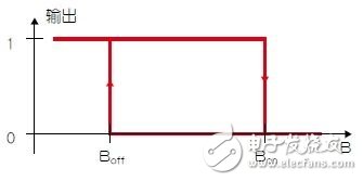
Figure 2: Static hysteresis loop of the Hall switch.
Between Bon and Boff, both output states are possible. In B "Bon", the output is definitely 0; before Boff, the switch will remain at 0; at Boff, the output becomes 1.
Threshold noise and minimum reliable hysteresis
There may be this question now: How small can the hysteresis loop be? To give an answer, the threshold noise effect must be considered. In fact, neither Bon nor Boff is a fixed threshold limited to a single value, which is affected by threshold noise caused by the thermal noise of the Hall sensor itself and other circuits, and these two values ​​become erratic. The noise level can be adjusted by design depending on current consumption and filter bandwidth. Noise is added to the threshold that is assumed to be constant. Now, Figure 3 shows the probability density function of Bon and Boff (not to scale).
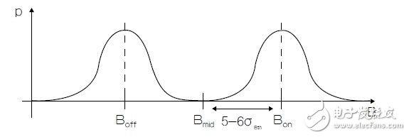
Figure 3: Probability density function of threshold noise
The height of the probability density is a measure of the likelihood of finding an instantaneous threshold under the condition of the corresponding flux density B. For thermal noise, the probability is a normal (Gaussian) distribution. The width of the density function is given by the standard deviation σBth, which is the same as the root mean square (RMS) noise value Bth, rms of the threshold.
Since the density cannot be zero, the tails of the probability density of Bon and Boff will always converge at the midpoint Bmid of Bon and Boff. This means that for a constant flux density Bmid, the Bon threshold may sometimes be (small probability) lower than Bmid, thus opening the switch. In addition, Boff may also be higher than Bmid, which in turn will turn off the switch. Thus, even for a constant magnetic flux density, the switch may begin to flip, which is generally undesirable. This phenomenon cannot be completely avoided, but the probability of its occurrence should be fully reduced. As a rule of thumb, if the difference of Bon-Boff is greater than or equal to 10~12σBth, this situation can be ignored.
Filtered sampling Hall switch
The signal processing of the HAL 15xy sensor family is based on a sampling design with a low pass filter. Thus, when a new sample of the filtered input is taken, the flipping of the switch output occurs only at certain equidistant points in time, for the HAL 15xy sensor, every 2 μs. Sampling jitter is caused when B passes through the flip threshold and is out of sync with the sample clock. Figure 4 shows a timing example of a filtered sampling switch (such as HAL 15xy):
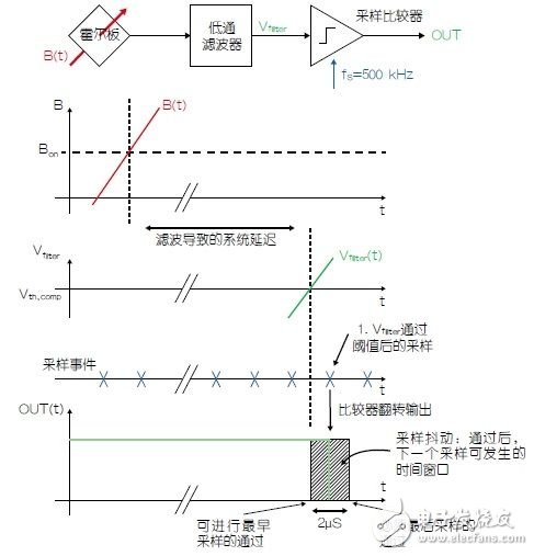
Figure 4: Delay of the filtered sampling Hall switch.
Here, it is assumed that the magnetic flux density B(t) completes a very fast transition when passing Bon to keep the threshold noise effect negligible at the moment. The Hall signal is proportional to B(t) and then passes through a low pass filter to eliminate higher bandwidth threshold noise.
It requires a constant system delay Δtsyst until the signal passing through the threshold passes through the filter, for example, Δtsyst here is 15~16μs. In addition, a random delay phase of up to 2 μs will occur until the next sample occurs and the comparator flips. When the Hall switch is repeatedly flipped, the random delay is called the sampling jitter Δtsampling.
Sampling jitter can be described by peak-to-peak or root mean square (RMS) values. The Δtsampling = ± 1 μs of the HAL 15xy sensor described by the peak-to-peak value during the 2 μs sampling interval. The probability of being discovered at all points in time is the same (probability distribution is shaped like a "box"). Thus, the typical value of RMS Δtsampling is 0.58 μs and the maximum value is 0.72 μs, which has better performance than competing products.
For the HAL 15xy series, the sample comparator is selected to operate at a 500 kHz sampling rate to ensure that typical sample jitter is reliably limited to ±1μs. This type of design supports dynamic compensation suppression in the comparator, which improves the overall accuracy of the magnetic threshold of the HAL 15xy sensor.
In addition, the sensor has a unique front-end design that allows for flexible definition of the low-pass filter bandwidth between 3kHz and 93kHz without the need to increase sampling jitter by programming with a metal mask. On the one hand, a smaller bandwidth increases the system delay of the signal path; on the other hand, it also reduces the threshold noise of the switch and improves the accuracy. The higher bandwidth situation is exactly the opposite of the above. Thanks to this feature, the HAL 15xy series can be customized for applications with fast dynamic or static magnetic field requirements.
Filterless sampling Hall switch
Hall switches such as Micronas' HAL 5xy series use a design without a filter IC. The unfiltered low-latency characteristics are attractive for fast response, depending on customer preferences, but at the expense of an increase in the noise threshold. For such a Hall switch, the sample jitter still exists, but since no filter is added, the system delay is gone. Figure 5 shows the general dynamic behavior of such a switch.
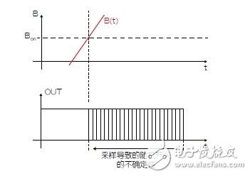
Figure 5: Delay of a sampled Hall switch without filtering.
This is why the peak-to-peak Δtsampling of the HAL 5xy sensor is randomly delayed, pp=±8μs, and the RMS value Δtsampling, rms.=±4.6μs. This comparison highlights the better performance of its successor product HAL 15xy from Micronas. .
HAL 15xy series switch jitter causes
The most interesting is the cause of the Hall switch jitter Δtswitch. The random distribution of switching delays - switching jitter, can be considered in accordance with Figure 8.
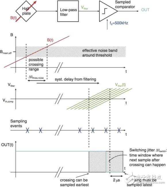
Figure 8: Switching jitter caused by threshold noise and sample jitter.
Hall plate: Hall plate
Low-pass filter: low pass filter
Sampled comparator: Sample Comparator
Possible crossing range: Possible range of passage
EffecTIve noise band around threshold: Effective noise band around the threshold
Syst. Delay from filtering: system delay caused by filtering
Sample events: sampling events
Sampling jitterâ–³tswitch: TIme window where next sample after crossing can
Happen: Sampling jitter Δtswitch: time window after the next sample can occur
Crossing can be sampled earliest: can pass the earliest sampling
Crossing must be sampled latest: must pass the last sample
Here, both threshold noise and sample jitter are present, resulting in combined switch jitter. B(t) slowly passes through the effective threshold, so the threshold noise can no longer be ignored. A noise band is drawn around the effective threshold. Figure 8 shows where the instantaneous threshold can be located. Within the noise band, the projection of B(t) on the time axis simply gives the timing jitter Δtthres.noise from the threshold noise. This timing jitter occurs when the filter output voltage Vfilter is delayed. Now, when the output is flipped, the resulting switching jitter contains jitter from threshold noise and always existing sample jitter.
Note that Figure 8 ignores the different probability densities from the two types of jitter, threshold noise and sample jitter, which in addition affect switching jitter. For high slopes, sample jitter dominates and can be used to estimate switching jitter. For low slopes, sampling jitter is also present, but effective threshold noise is dominant.
By setting the sampling jitter Δtsampling, rms=Bth, rms jitter (threshold noise introduction), the boundary between the high and low slopes can be easily found.

Therefore, when the rate of magnetic change is much lower than 124 mT/ms, the resulting switching jitter can be evaluated only from the jitter of the threshold noise, and the sampling jitter is negligible.
in conclusion
There are two sources of jitter in the Hall switch. First, the thermal noise of the Hall plate and the threshold noise caused by signal processing; second, the sampling results in system-specific sampling jitter. With the optimized configuration of Micronas' proprietary technology, the HAL 15xy sensor family operates at very high sampling frequencies, so the resulting sample jitter is very small. This new and optimized circuit design maintains low power consumption while maintaining extremely low thermal noise, with the best noise performance of its class. In addition, the bandwidth of the analog filter can be reduced or increased by metal mask programming, making it possible to minimize noise or delay time.
Female Header Connector,Single Row Female Header Connector,U-Type Female Header Connector,Single Row U Female Header Connector
Dongguan Yangyue Metal Technology Co., Ltd , https://www.yyconnector.com