Board design is a critical and time-consuming task, and any problem requires engineers to examine the entire design on a network-by-component basis. It can be said that the design requirements of the board are as good as the chip design.
A typical board design flow consists of the following steps:

The first three steps take the most time because the schematic check is a manual process. Imagine a SoC board with 1000 or more connections. Manually checking each connection is a tedious task. In fact, it is almost impossible to check each connection, which can lead to problems with the final board, such as incorrect wiring, floating nodes, and so on.
The schematic capture phase generally faces the following types of problems:
â— Underscore error: such as APLLVDD and APLL_VDD
â— Capitalization issues: such as VDDE and vdde
â—Spelling mistakes
â—Signal short circuit problem
â—...and many more
To avoid these errors, there should be a way to check the complete schematic in a matter of seconds. This method can be implemented with schematic simulation, which is rarely seen in the current board design flow. Schematic simulation allows you to see the final output at the desired node, so it automatically checks for all connection problems.
The following is explained by a project example. Consider a typical block diagram of a board:

figure 1
In complex board designs, the number of connections can reach thousands, and very few changes are likely to waste a lot of time checking.
Schematic simulation not only saves design time, but also improves board quality and increases overall process efficiency.
A typical device under test (DUT) has the following signals:

figure 2
The device under test will have various signals after some pre-adjustment, and there are various modules, such as voltage regulators, op amps, etc., for signal adjustment. Consider an example of a power supply signal obtained by a voltage regulator:

Figure 3: Schematic of the sample board.
In order to verify the connection and perform an overall check, a schematic simulation was used. Schematic simulation consists of schematic creation, test platform creation, and simulation.
During the test platform creation process, an excitation signal is sent to the necessary input, and then the output is observed at the signal point of interest.
The above process can be implemented by connecting a probe to a node to be observed. The node voltage and waveform can indicate if there is an error in the schematic. All signal connections are automatically checked.

Figure 4: Schematic test platform and simulation values ​​for each node.
Let's take a look at a part of the above picture where the nodes and voltages detected are clearly visible:

So with the help of simulation, we can directly observe the results and confirm that the schematic of the board is correct. In addition, a survey of design changes can be made by carefully adjusting the stimulus signal or component values. Schematic simulation can therefore save board design and inspectors a lot of time and increase the chances of design correctness.
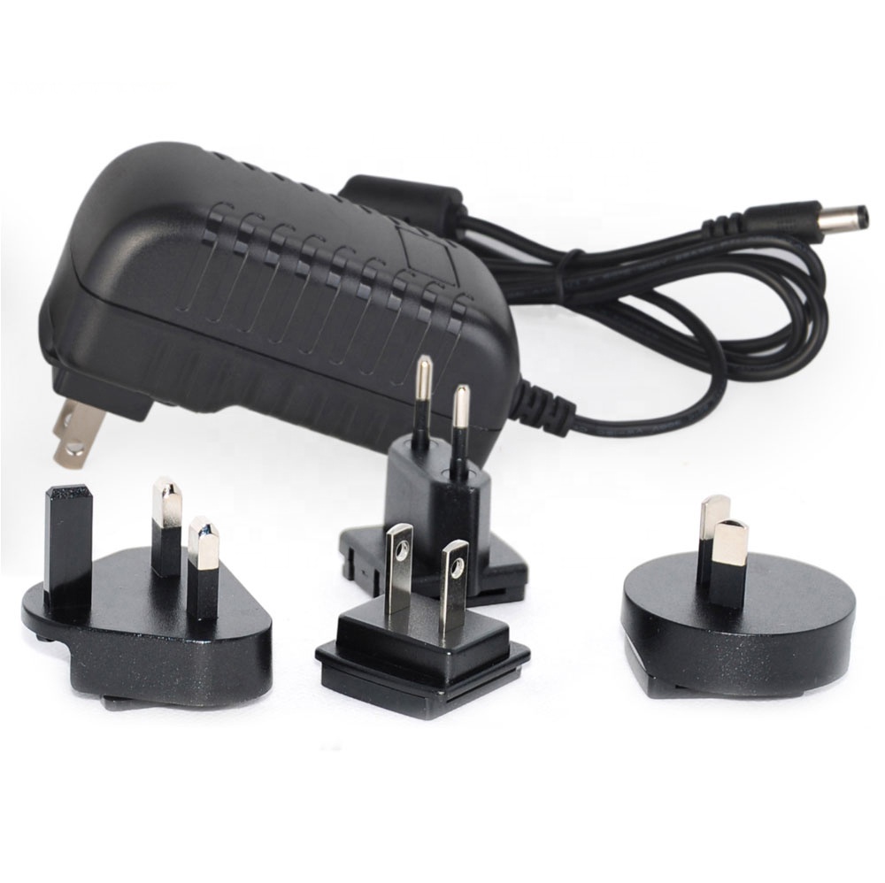
5V Switching Wall Charger Power Adapter for Home Electronics

Micro USB:
Original back-and-white display Kindle 1st Gen, Kindle Fire Kindle HD Fire HD 6 8 10 HDX 7 8.9 9.7, Samsung Galaxy S7/Edge, S6/Edge, S5, S4, S3, S2, Si9003, S5820, N7100, Note3, Note4
5.5mm x 2.1mm:
For Bluetooth speakers/ Electronic Toys/ Mini Fan/ Portable Air Conditioner/ LED Pixel Light/ Monitor/ Camera/ Webcam Router/ Cable Modem/ USB-HUB/ photo player/ SCM development/ access control attendance ect.
4.0mm x 1.7mm:
For mp3 mp4 speaker CCTV camera power supply connection/ digital picture frame/ shower Christmas lights/ Sabrent USB HUB/ digital recorder ect.
3.5mm x 1.35mm:
* For Facial Cleansing Brush: Foreo Luna 3/ Luna 3 Plus/ Luna/ Luna2/ Luna Mini/ Luna Mini 2/ Luna Go/ Luna Luxe, ISSA Series E-Toothbrush ISSA / ISSA Hybrid / ISSA mini / ISSA Mikro / ISSA play, ESPADA Acne Treatment Device, IRIS Eye Massager
* For Fairywill Sonic Electric Toothbrush FWP11 FW507 FWD1 FWD3 FWD8 FW917 FW2001 FWE11 FWE11 FW917 FWT9 ect.
* For LELO Ida, Lyla, Lyla 2, Oden, Oden 2, Ora, Ora 2, Tara, Alia, Isla, Soraya, Inez, Yva, Mia, Mia 2, Nea, Nea 2, Lily, Lily 2, Liv, Liv 2, Gigi, Gigi 2.
* For LELO Mona, Mona 2, Mona Wave, Ina, Ina 2, Ina Wave, Siri, Siri 2, Iris, Elise, Elise 2, Billy, Tor, Tor 2, Bo, Hugo, Bruno, Hula Beads, Loki, Loki Wave.
5v wall charger,5v 2a wall charger,5v 3a wall charger,5v power charger,switching 5v charger,5v 1a Wall Wart Transformer Charger,5v 2a Wall Wart Transformer Charger,5v 3a Wall Wart Transformer Charger,5V 2A/2000mah AC Power Adapter Adaptor Wall Charge
Shenzhen Waweis Technology Co., Ltd. , https://www.waweis.com